Methods of forming nanosheet transistor with dielectric isolation of source-drain regions and related structure

Active Publication Date: 2018-04-17
GLOBALFOUNDRIES US INC
View PDF13 Cites 77 Cited by
  • Summary
  • Abstract
  • Description
  • Claims
  • Application Information

AI Technical Summary

Benefits of technology

[0007]A third aspect of the disclosure provides a method of forming an integrated circuit (IC) structure, the method including: forming a first pair of transistor sites and a second pair of transistor sites from a substrate, wherein a lateral separation distance between the first pair of transistor sites is less than a separation distance between the second pair of transistor sites, and wherein each of the first pair of transistor sites and the second pair of transistor sites includes a pair of nanosheet stacks each positioned on a respective one of the pair of transistor sites, and a pair of gate structures each positioned on a respective one of the pair of transistor sites; selectively forming an insulative region between the first pair of transistor sites to cover a first portion of

Problems solved by technology

A number of challenges arise as feature sizes of FETs and ICs get smaller.
For example, significant downsizing of conventional planar FETs may produce electrostatic issues and electron mobility degradation.
Scaled-down planar FETs may have shorter gate lengths that make it more difficult to control the channel.
Differences in structure between nanosheet transistors and conventional transistor structures, and the processing needed to form nanosheet transistors, may be associated with differences in performance during operation.
Such effects on performance can be difficult to manage in structures which include varying sep

Method used


Image

  • Methods of forming nanosheet transistor with dielectric isolation of source-drain regions and related structure
  • Methods of forming nanosheet transistor with dielectric isolation of source-drain regions and related structure
  • Methods of forming nanosheet transistor with dielectric isolation of source-drain regions and related structure

Examples


Embodiment Construction

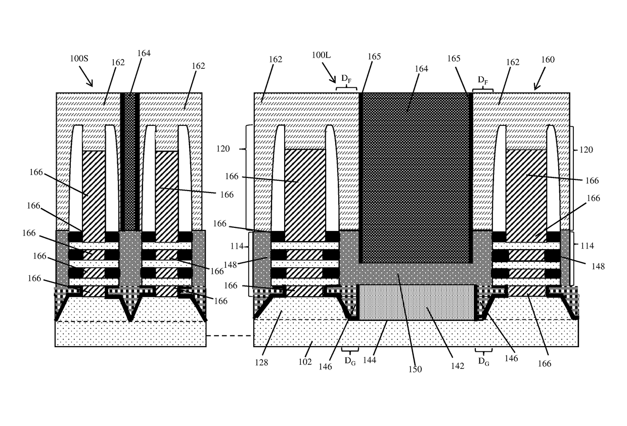
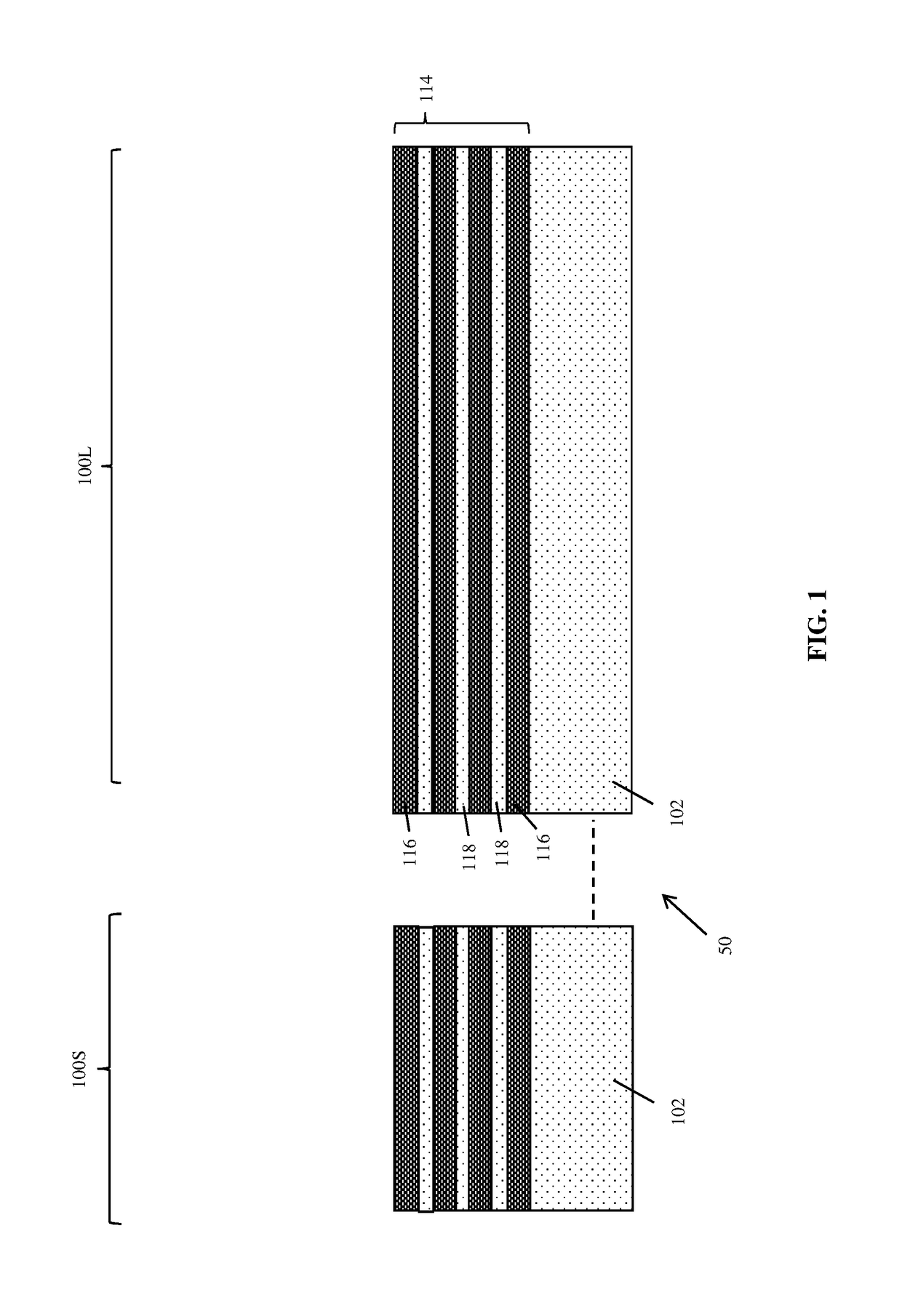
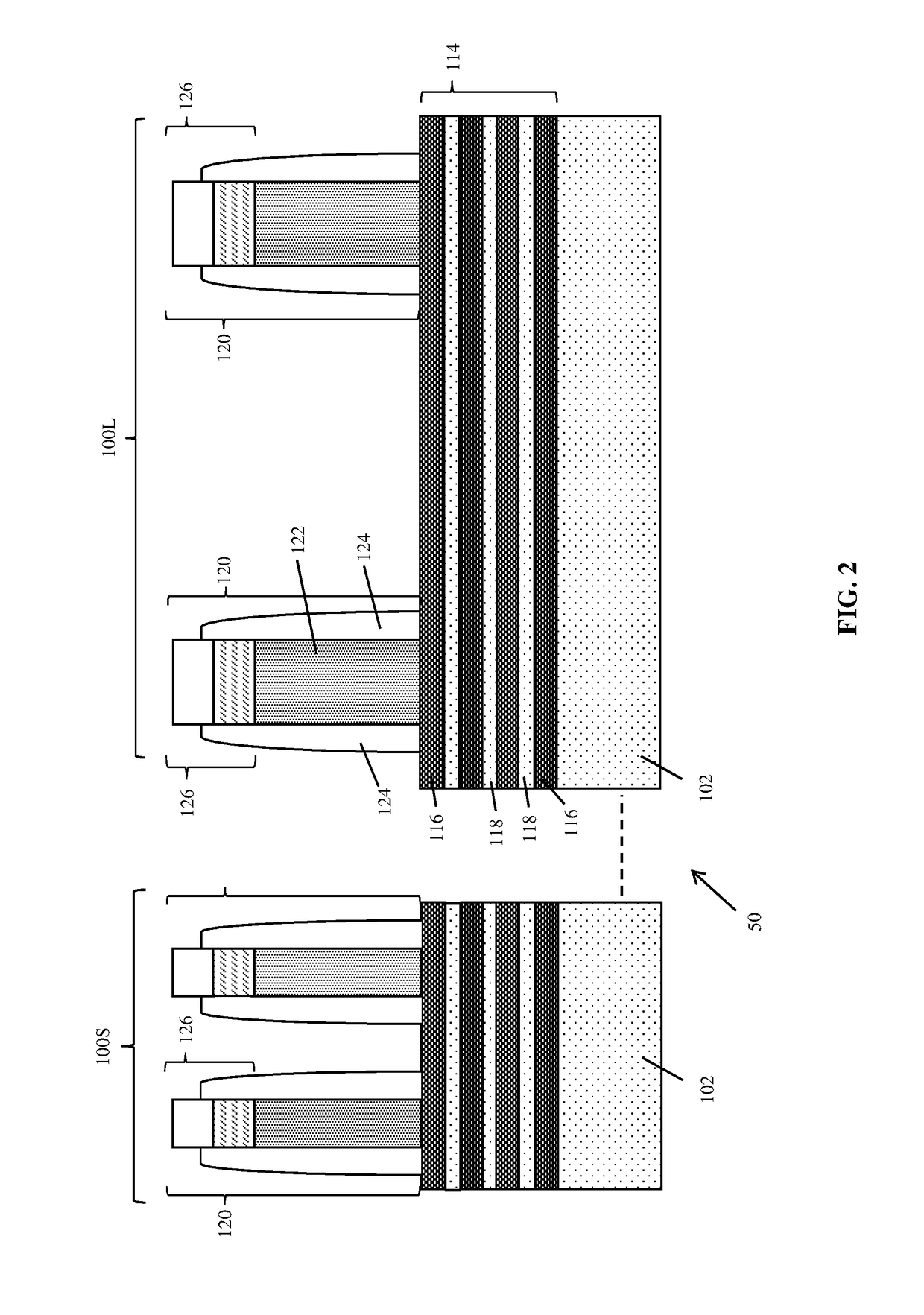
[0035]The present disclosure relates to integrated circuit (IC) design, and more particularly to IC structures which include (“nanosheet transistors”) using bottom dielectric isolation of the source and drain contacts, and methods of forming the same. Specifically, the present disclosure provides for various IC structures with insulative dielectric materials physically and electrically separating source and drain contacts from the substrate, and methods of forming the same. In a nanosheet transistor structure, electrical connection with the various nanosheets in a gate region acting as transistor channel may be provided through a semiconductive source / drain epitaxial region grown from the edges of the semiconductor nanosheets. The source / drain epitaxial regions formed in embodiments of the present disclosure may be positioned over dielectric material formed for processing consistency in multiple regions, and to provide physical and electrical separation from the substrate. The vario...


PUM


Abstract

An IC structure according to the disclosure includes: a substrate; a pair of transistor sites positioned on the substrate, wherein an upper surface of the substrate laterally between the pair of transistor sites defines a separation region; a pair of nanosheet stacks, each positioned on one of the pair of transistor sites; an insulative liner conformally positioned on the upper surface of the substrate within the separation region, and a sidewall surface of each of the pair of transistor sites; a semiconductor mandrel positioned on the insulative liner and over the separation region; a pair of insulator regions each positioned laterally between the semiconductor mandrel and the insulative liner on the sidewall surfaces of each of the pair of transistor sites; and a source/drain epitaxial region positioned over the pair of insulator regions and the semiconductor mandrel, wherein the source/drain epitaxial region laterally abuts the pair of nanosheet stacks.

Description

BACKGROUNDTechnical Field[0001]The present disclosure relates to integrated circuit (IC) design, and more particularly to IC structures based on electrically isolated stacked nanosheet Field Effect Transistor structures using bottom dielectric isolation of the Source and Drain contacts, and methods of forming the same.Related Art[0002]A nanosheet transistor refers to a type of field-effect transistor (FET) that includes a plurality of stacked nanosheets extending between a pair of source / drain epitaxial regions. FETs typically include doped source / drain epitaxial regions that are formed in a semiconductor substrate and separated by a channel region. A gate insulation layer is positioned above the channel region and a conductive gate electrode is positioned above the gate insulation layer. The gate insulation layer and the gate electrode together may be referred to as the “gate stack,”“gate structure,” etc., for the device. By applying an appropriate voltage to the gate electrode, th...

Claims


Application Information

Patent Timeline
IPC IPC(8): H01L21/84H01L21/8234H01L27/088H01L29/45H01L29/786H01L29/423
CPCH01L29/78696H01L29/42392H01L29/458H01L27/088H01L21/823412B82Y40/00H01L29/0684H01L29/0847H01L29/66795H01L29/785H01L29/66431H01L29/775H01L29/778H01L29/165B82Y10/00H01L29/41725H01L29/66439H01L29/0653H01L29/0673H01L21/823418H01L21/823468H01L29/66545
Inventor FROUGIER, JULIENSUNG, MIN GYUXIE, RUILONGPARK, CHANROBENTLEY, STEVEN
Owner GLOBALFOUNDRIES US INC
Why Eureka
Try Eureka