Method for assembling a microelectronic chip element on a wire element, and installation enabling assembly to be performed

a technology of microelectronic chip elements and wire elements, which is applied in the direction of basic electric elements, solid-state devices, electric apparatus, etc., can solve the problems of unfavorable flexible structure integration, unfavorable chip element handling and association, and particularly rigid mechanical support, etc., to facilitate the fabrication of a daisy chain and low cost

Active Publication Date: 2018-04-24
COMMISSARIAT A LENERGIE ATOMIQUE ET AUX ENERGIES ALTERNATIVES
View PDF22 Cites 0 Cited by
  • Summary
  • Abstract
  • Description
  • Claims
  • Application Information

AI Technical Summary

Benefits of technology

[0005]It is thus sought to facilitate fabrication of a daisy chain comprising microelectronic chip elements, at low cost.
[0021]Advantageously, during the fixing step of the wire element onto the connection terminal, the wire element is securedly held against the material by biasing said wire element in the direction of the bump and heating the wire element to soften the material.

Problems solved by technology

It does however have the main drawback of using a rigid mechanical support which is particularly unsuitable for integration in flexible structures.
The chip elements are electrically connected to one another via a wire element before being finally separated from one another, the whole operation being performed on the silicon wafer, which does not facilitate handling and association of a chip element with the wire element.

Method used


Image

  • Method for assembling a microelectronic chip element on a wire element, and installation enabling assembly to be performed
  • Method for assembling a microelectronic chip element on a wire element, and installation enabling assembly to be performed
  • Method for assembling a microelectronic chip element on a wire element, and installation enabling assembly to be performed

Examples


Embodiment Construction

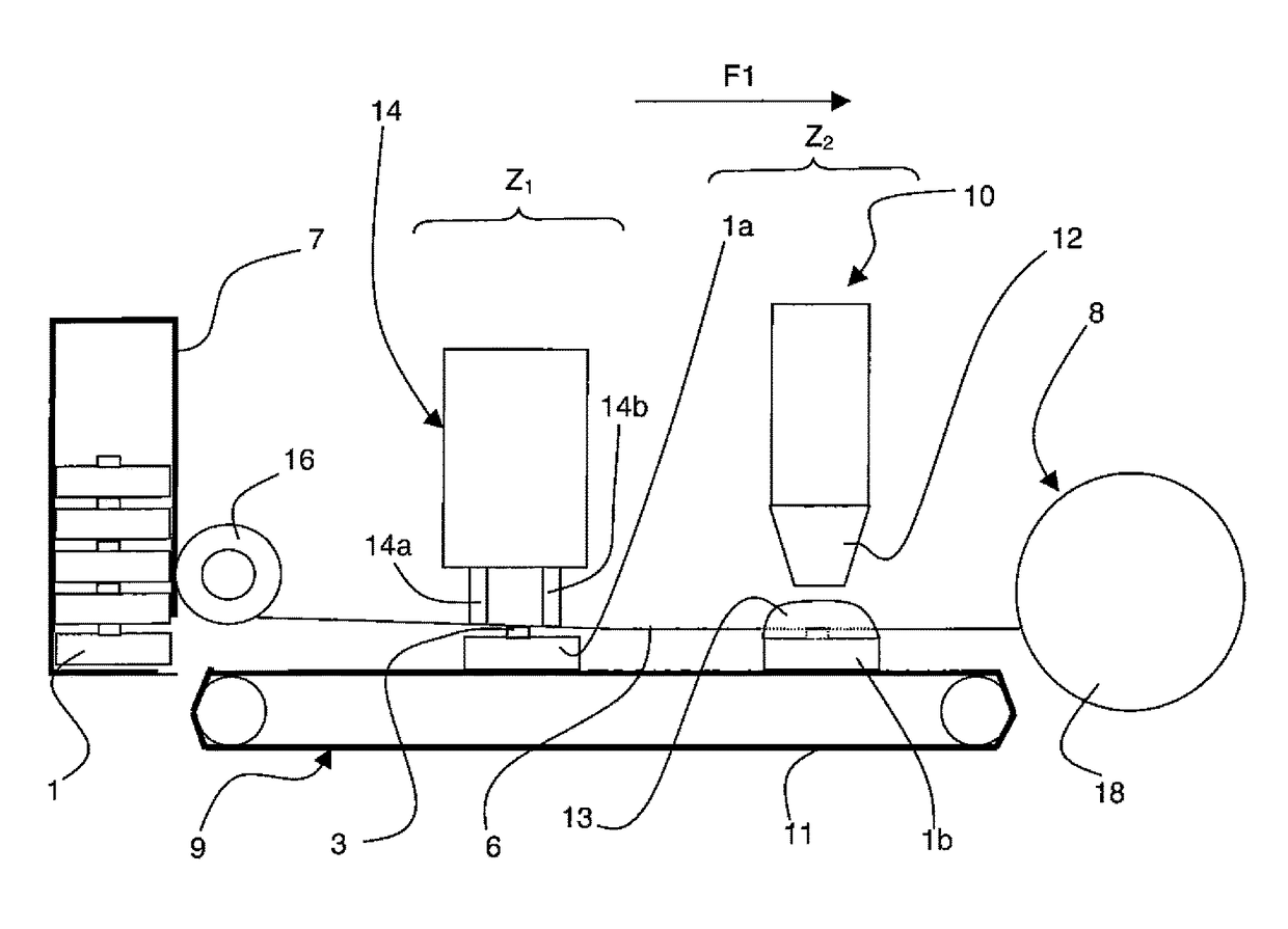
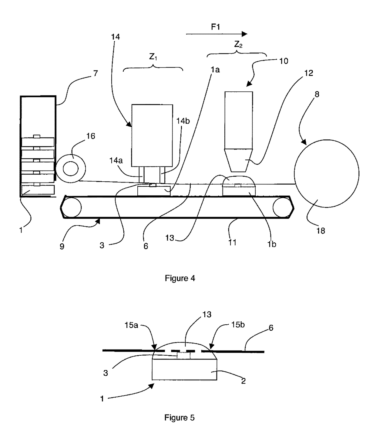
[0041]As indicated in the foregoing, it is sought to advantageously produce a daisy chain having a base formed by a series of microelectronic chip elements (or at least one chip element) assembly of which is solidified by addition of coating material forming the cover.

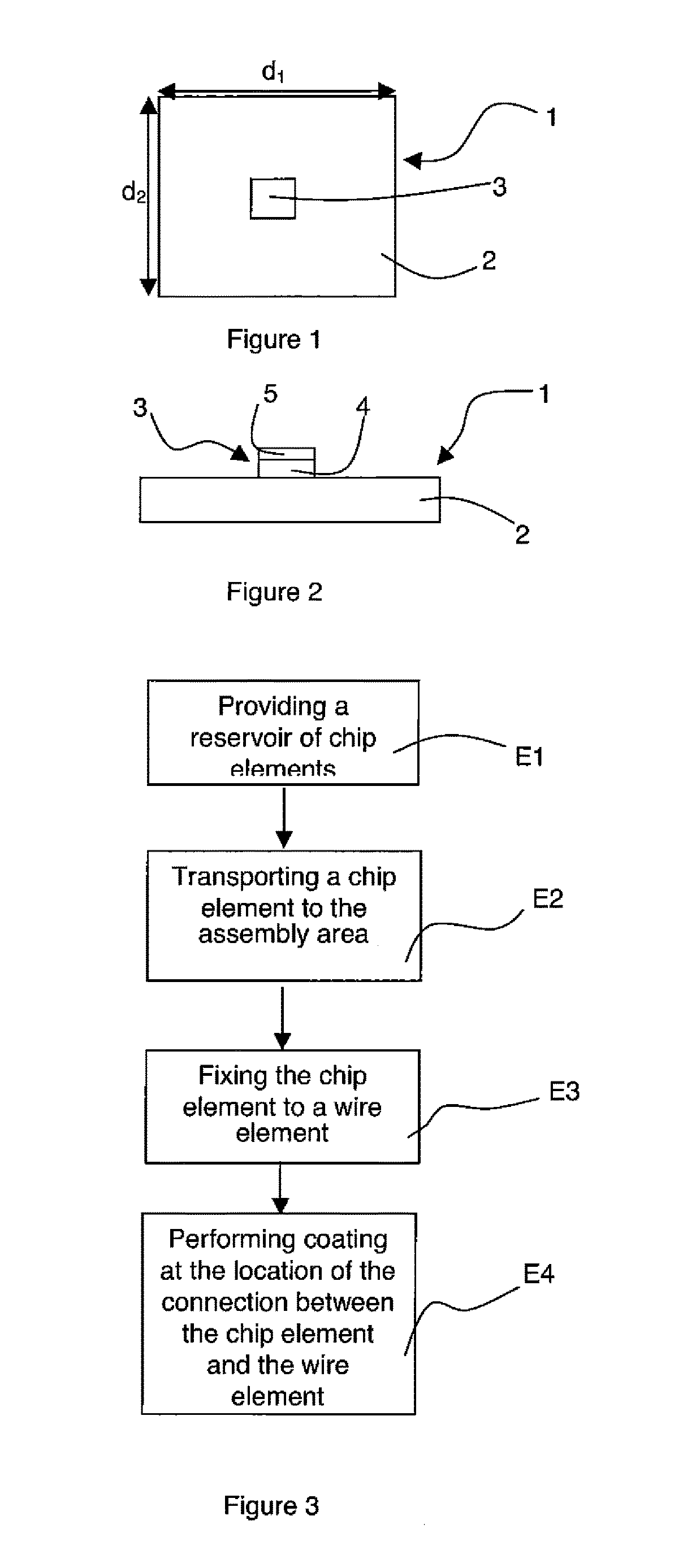
[0042]An example of a microelectronic chip element able to be used in the scope of the present invention is visible in FIGS. 1 and 2. Such a microelectronic chip element 1 can comprise a base 2 containing for example the chip or constituting the chip, and a connection terminal 3 advantageously salient from the external surface of base 2.

[0043]According to a particular embodiment, base 2 of chip element 1 is of substantially parallelepipedic shape. Connection terminal 3 is salient from one of the surfaces of base 2, advantageously from a surface called main surface. The main surface is defined as the surface having the largest lateral dimensions d1 and d2, in other words it is the surface having the largest surface area...


PUM


Abstract

Method for assembling includes: providing a system to transfer wire element from wire element supply device to wire element storage device; stretching wire element between supply and storage devices by tensioning; providing an individualized reservoir and separated chip elements, each including a connection terminal including a top with free access facing in which chip element is not present; transporting the chip element from reservoir to an assembly area between supply and storage devices in which wire element is tightly stretched in assembly area; fixing electrically conducting wire element to chip element connection terminal in assembly area; and adding electrically insulating material on chip element after latter has been fixed to wire element forming a cover, the addition of material being performed on surface of chip element including connection terminal fixed to wire element to cover at least the connection terminal and portion of wire element at fixing point of latter.

Description

BACKGROUND OF THE INVENTION[0001]The invention relates to a method for assembling a microelectronic chip element on an electrically conducting wire element.State of the Art[0002]Numerous techniques exist at the present time to mechanically and electrically connect microelectronic chip elements to one another. A conventional technique consists in making a rigid mechanical connection between the chip elements, once the latter have been formed on a substrate and released by dicing. The chip elements, which are then fixed on a rigid support, are then electrically connected before a protective coating is formed. This approach, consisting in making the connection on a rigid support, is conventionally used when a great complexity in connection of the chip elements exists. It does however have the main drawback of using a rigid mechanical support which is particularly unsuitable for integration in flexible structures.[0003]The document WO2009 / 013409 filed by the applicant describes the use ...

Claims


Application Information

Patent Timeline
Patent Type & Authority Patents(United States)
IPC IPC(8): H05K13/02H05K13/06H05K13/00H01L23/00
CPCH01L24/85H01L24/06H01L24/78H01L2933/0066H01L2924/181H01L2924/12042H01L2924/12041H01L2924/00014H01L2224/85862H01L2224/85805H01L2224/85801H01L2224/85375H01L2224/85205H01L2224/8592H01L2224/78651H01L2224/78611H01L2224/7898H01L2224/4918H01L24/05H01L24/45H01L24/48H01L24/49H01L2224/04042H01L2224/0569H01L2224/05601H01L2224/0618H01L2224/45099H01L2224/4847H01L2924/014H01L2924/00
Inventor BRUN, JEAN
Owner COMMISSARIAT A LENERGIE ATOMIQUE ET AUX ENERGIES ALTERNATIVES
Why Eureka
Try Eureka