Direct current pulsing plasma systems

a plasma system and direct current technology, applied in the field ofplasma processing systems, can solve the problems of adding complexity and cost to the power supply of the pulsed rf power supply

Active Publication Date: 2018-05-08
LAM RES CORP
View PDF3 Cites 14 Cited by
  • Summary
  • Abstract
  • Description
  • Claims
  • Application Information

AI Technical Summary

Benefits of technology

[0014]In some embodiments, the dynamic adjustment of the rectifier circuit enables settings of higher or lower amplitudes during each active pulse of the pulsing pattern.

Problems solved by technology

Although pulsing of the RF power supply has shown improvement in the resulting process, pulsing RF power supplies does add complexity and cost.

Method used


Image

  • Direct current pulsing plasma systems
  • Direct current pulsing plasma systems
  • Direct current pulsing plasma systems

Examples


Embodiment Construction

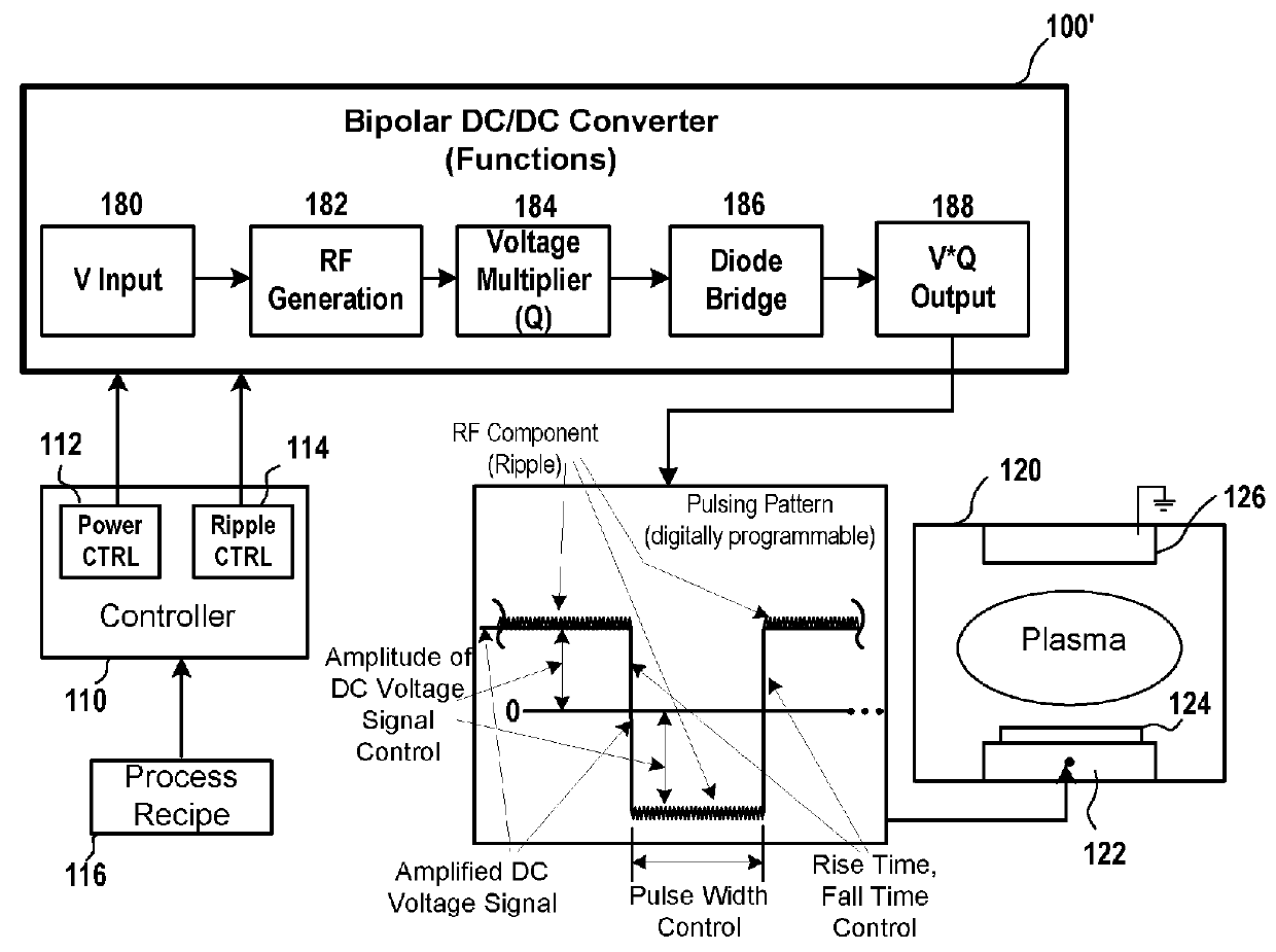
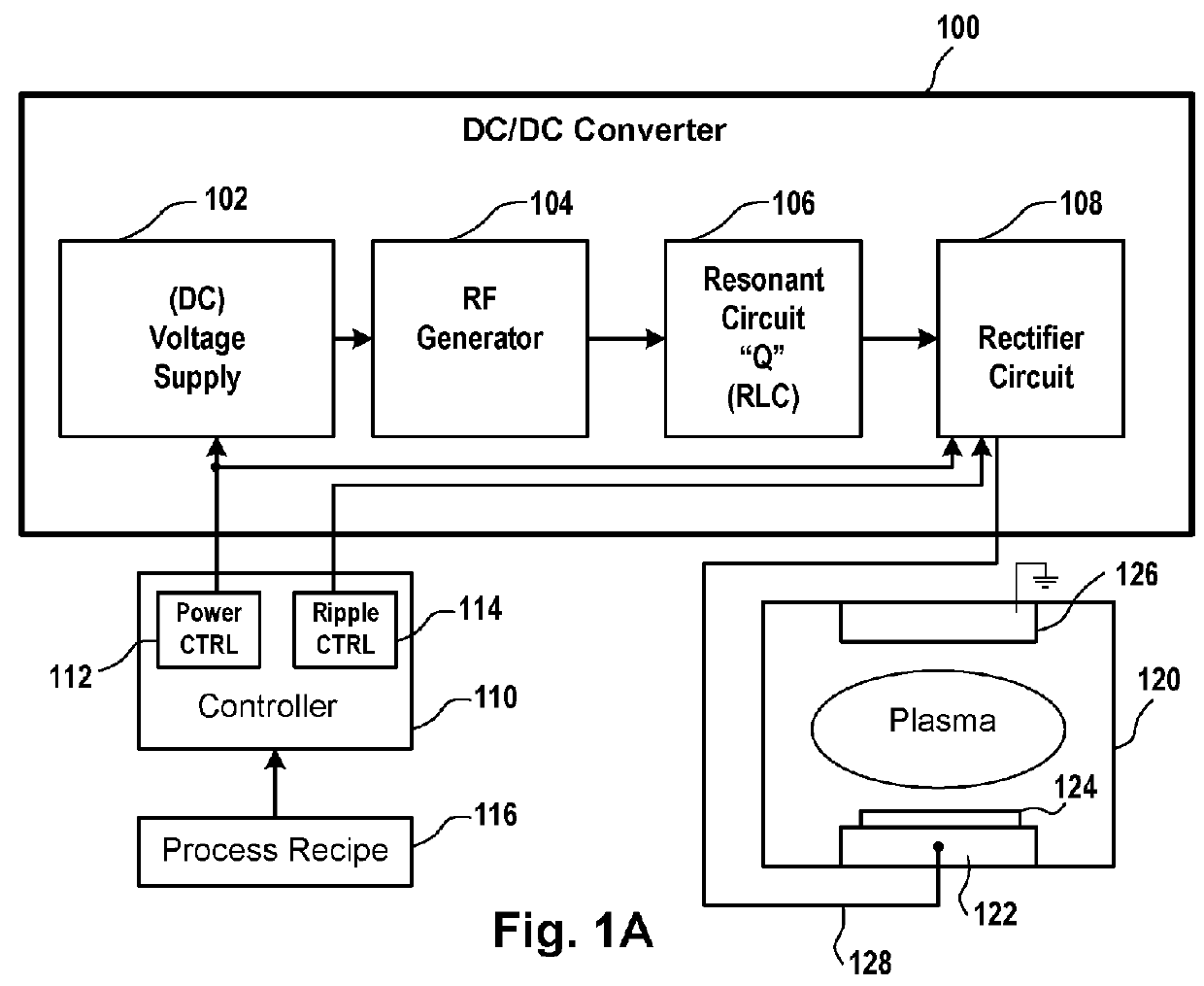
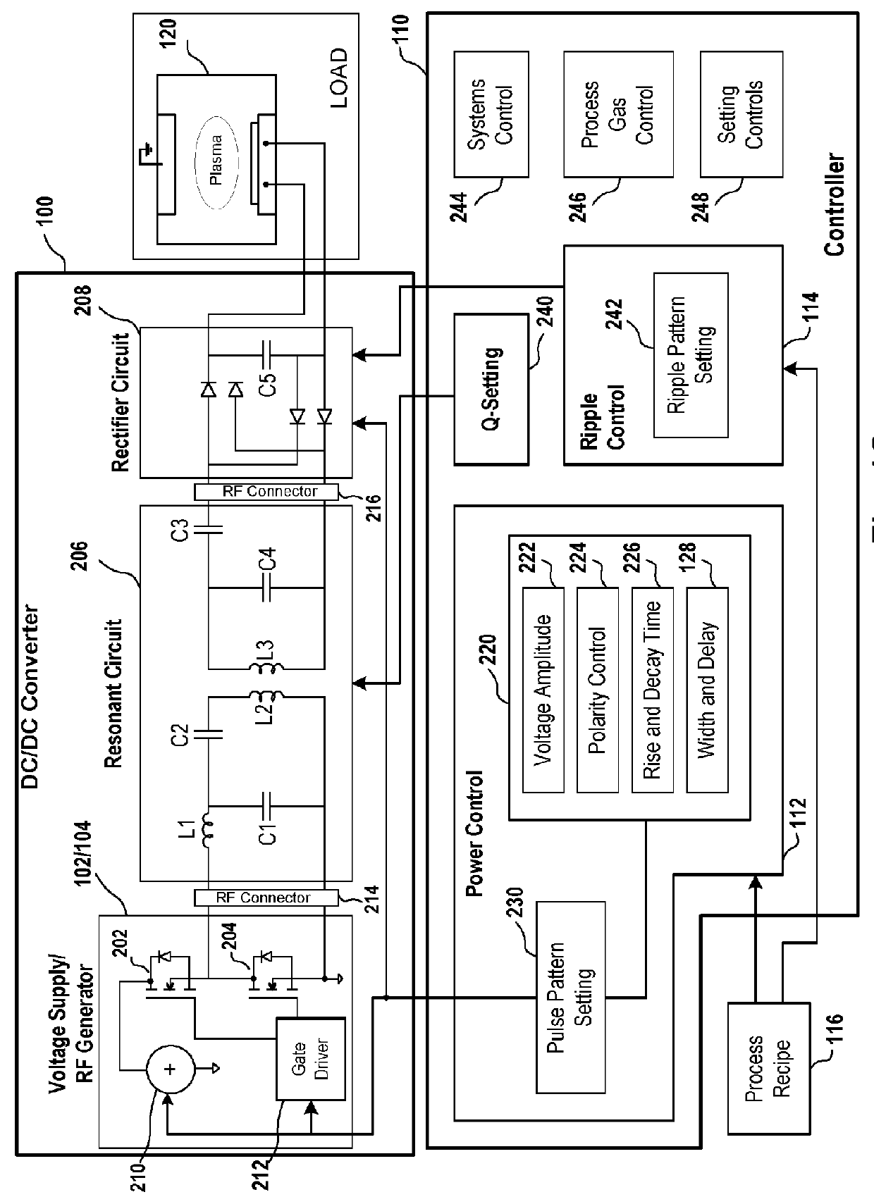
[0037]The following embodiments describe methods, devices, systems, and computer programs for a DC / DC power converter for supplying pulsed power to an electrode of a plasma processing system.

[0038]In one embodiment, a method is disclosed where a high voltage from a DC power supply is applied to a plasm a processing system with the positive and negative pulses being independently controlled in voltage amplitude, polarity, rise and decay time, width and delay. The DC pulses are provided, as disclosed below, with a RF component ripple.

[0039]In processing plasmas, it is useful to have a controlled ion bombardment onto the substrate containing features being etched to ultimately define the microelectronic circuits being processed. This is pertinent to both the positive ions which are commonly used to sputter etch very small holes and to densify growing films and to the negative ions which can enter the holes being etched and neutralize the positive charge accumulation. As the plasma itse...


PUM


Abstract

A plasma processing system is provided that includes a chamber having a lower electrode coupled to a substrate support and an upper electrode coupled to ground. The plasma processing system having a plasma processing volume that is defined between the upper electrode and the lower electrode. A direct current (DC) to direct current (DC) converter is provided to receive at an input a DC voltage input and supply at an output an amplified DC voltage signal that includes a radio frequency (RF) component. The DC voltage input follows a pulsing pattern that is digitally programmable. The output of the DC to DC convertor is connected to the lower electrode of the chamber. A controller is interfaced with the DC to DC converter to set the pulsing pattern. In one example, the DC to DC converter uses one of a bipolar or non-bipolar DC voltage supply and a RF generator is driven by a DC voltage supply. The RF generator is configured to produce a frequency ripple that defines the RF component.

Description

CLAIM OF PRIORITY[0001]This application claims priority from U.S. Provisional Patent Application No. 62 / 301,591 filed on Feb. 29, 2016, entitled, “Direct Current Pulsing Plasma Systems”, of which is herein incorporated by reference.BACKGROUND[0002]1. Field of the Invention[0003]The present embodiments relate to plasma processing systems, and in particular, to plasma processing systems that utilize direct current (DC) pulsing as the power source.[0004]2. Description of the Related Art[0005]Plasma has long been employed to process substrates (e. g., semiconductor wafers, flat panels, etc.) to form electronic products (e.g., integrated circuits, flat panel displays, etc.). Semiconductor wafers are typically placed in an etch chamber with a photoresist mask layer to selectively etch the underlying materials. The etching process removes the underlying materials (metals and / or dielectrics) not covered by the photoresist. The etching process, along with other processing operations, is repe...

Claims


Application Information

Patent Timeline
Patent Type & Authority Patents(United States)
IPC IPC(8): H01J7/24H01J37/32H02M3/335H02M1/14H01L21/3065
CPCH01J37/32091H01J37/32174H01L21/3065H02M3/33507H02M1/14H01J37/32146H01J37/32082H01J9/00H01J37/32798H01J37/32807H01J37/32889H01J2237/30H02M1/0058Y02B70/10H01J37/32532H05H1/46
Inventor BOSWELL, RODERICK W.GOTTSCHO, RICHARD ALAN
Owner LAM RES CORP
Why Eureka
Try Eureka