Electrode, ferroelectric ceramics and manufacturing method thereof
a technology of ferroelectric ceramics and manufacturing methods, applied in vacuum evaporation coatings, chemistry apparatuses and processes, coatings, etc., can solve the problems of increasing cost and the requirement of electrodes with cost lower than those of pt films, and achieve excellent piezoelectric properties
- Summary
- Abstract
- Description
- Claims
- Application Information
AI Technical Summary
Benefits of technology
Problems solved by technology
Method used
Image
Examples
example 1
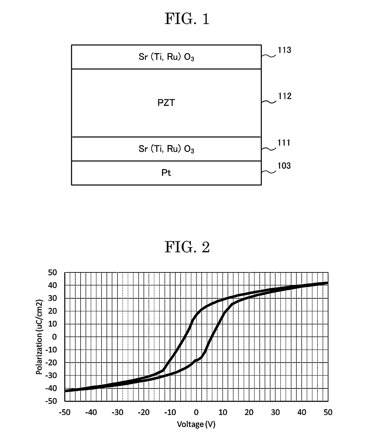
[0066]FIG. 2 is a drawing showing a result of evaluating hysteresis of a PZT film of a sample 2 in Example 1. In FIG. 2, the vertical axis shows polarization (μC / cm2), and the horizontal axis shows an applied voltage (V).
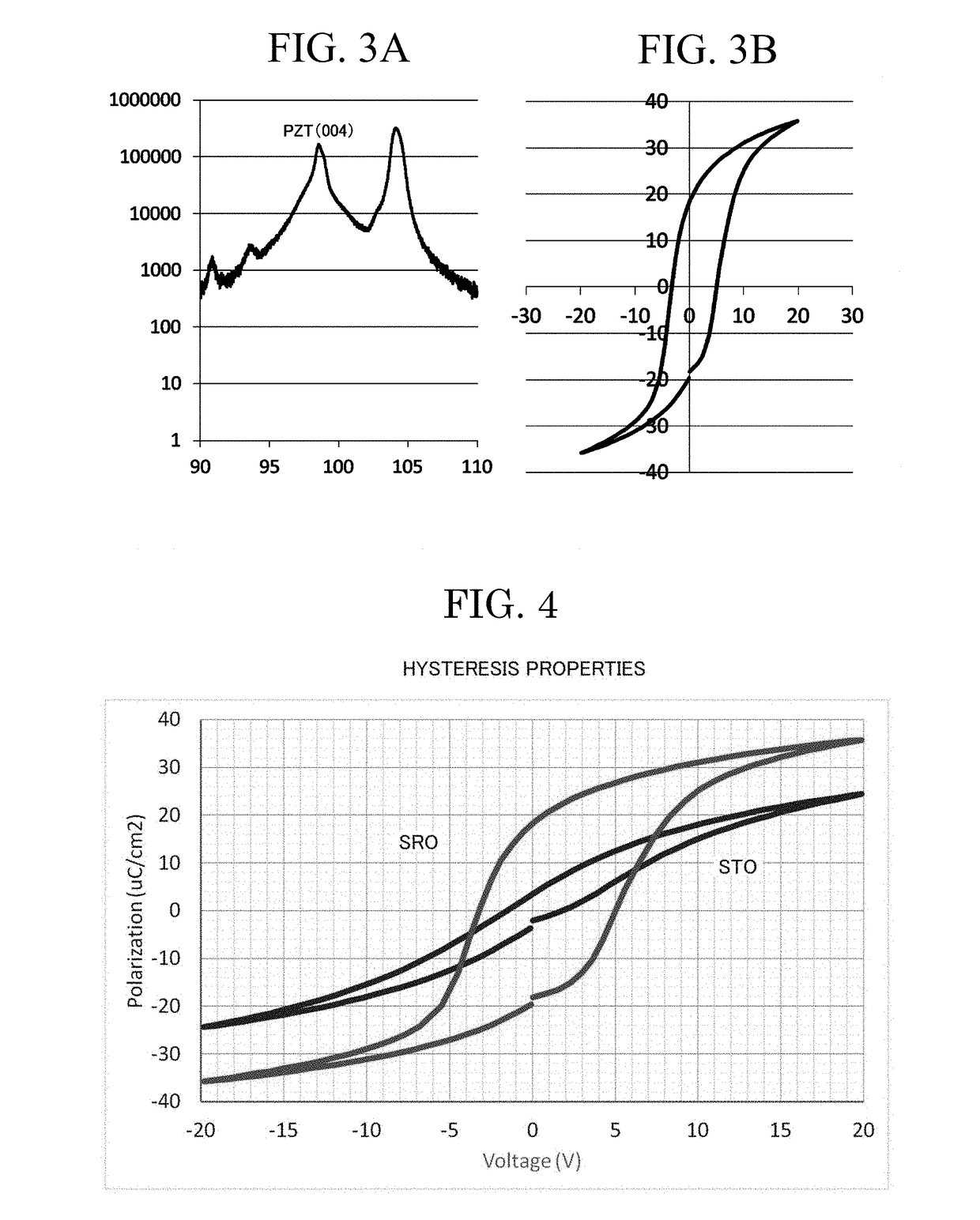
[0067]FIG. 3A is a chart showing a result of XRD of the PZT film of the sample 2 in Example 1, and FIG. 3B is a drawing showing a result of evaluating hysteresis of the PZT film of the sample 2 in Example 1.
[0068]Hereinafter, a production method of samples 1 and 2 in the Example will be explained.
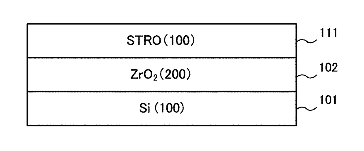
[0069]A ZrO2 film oriented in (200) was formed on a Si wafer having a (100) crystal plane by a reactive evaporation method, and a Pt film oriented in (200) was formed on the ZrO2 film by sputtering. Processes up to this process are common to samples 1 and 2.
[0070]Next, a first Sr(Ti0.8Ru0.2)O3 film was formed on the Pt film of the sample 1 by sputtering. Furthermore, a first Sr(Ti0.95Ru0.05)O3 film was formed on the Pt film of the sample 2 by sputtering. Conditions of the s...
example 2
[0130]FIG. 7A is a cross-sectional view of a sample after the following wet-etching of and the peeling of the PZT film of the same sample (PZT / Sr(Ti0.8Ru0.2)O3(STRO) / Pt) as the sample 1 in Example 1, and FIG. 7B is a cross-sectional view of a sample after the following wet-etching of and the peeling of the PZT film of the sample (PZT / Pt) in Comparative Example 2.
[0131][0132]10 w %-HCl+0.1 w %-HF aqueous solution[0133]wet-etching of PZT capacitor obtained by coating resist having a thickness of 1 μm[0134]Use amount of etchant of 50 ml, 35° C.[0135]Approximately 100 seconds at 700 rpm of ACT-300AII[0136]SEM observation and evaluation after washing with water
[0137]As shown in FIG. 7B, when the Sr(Ti0.8Ru0.2)O3 film (STRO) is not sandwiched on and under a PZT film, the PZT film remains at the interface with the Pt film even when wet-etching is performed. In contrast to this, as shown in FIG. 7A, when the Sr(Ti0.8Ru0.2)O3 film (STRO) is sandwiched on and under a PZT film, the PZT film is...
PUM
| Property | Measurement | Unit |
|---|---|---|
| thickness | aaaaa | aaaaa |
| thickness | aaaaa | aaaaa |
| thickness | aaaaa | aaaaa |
Abstract
Description
Claims
Application Information


