

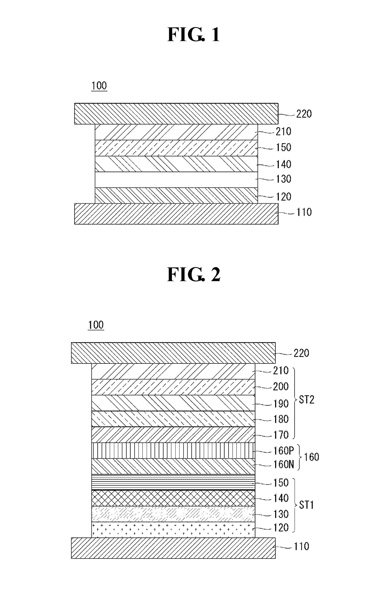
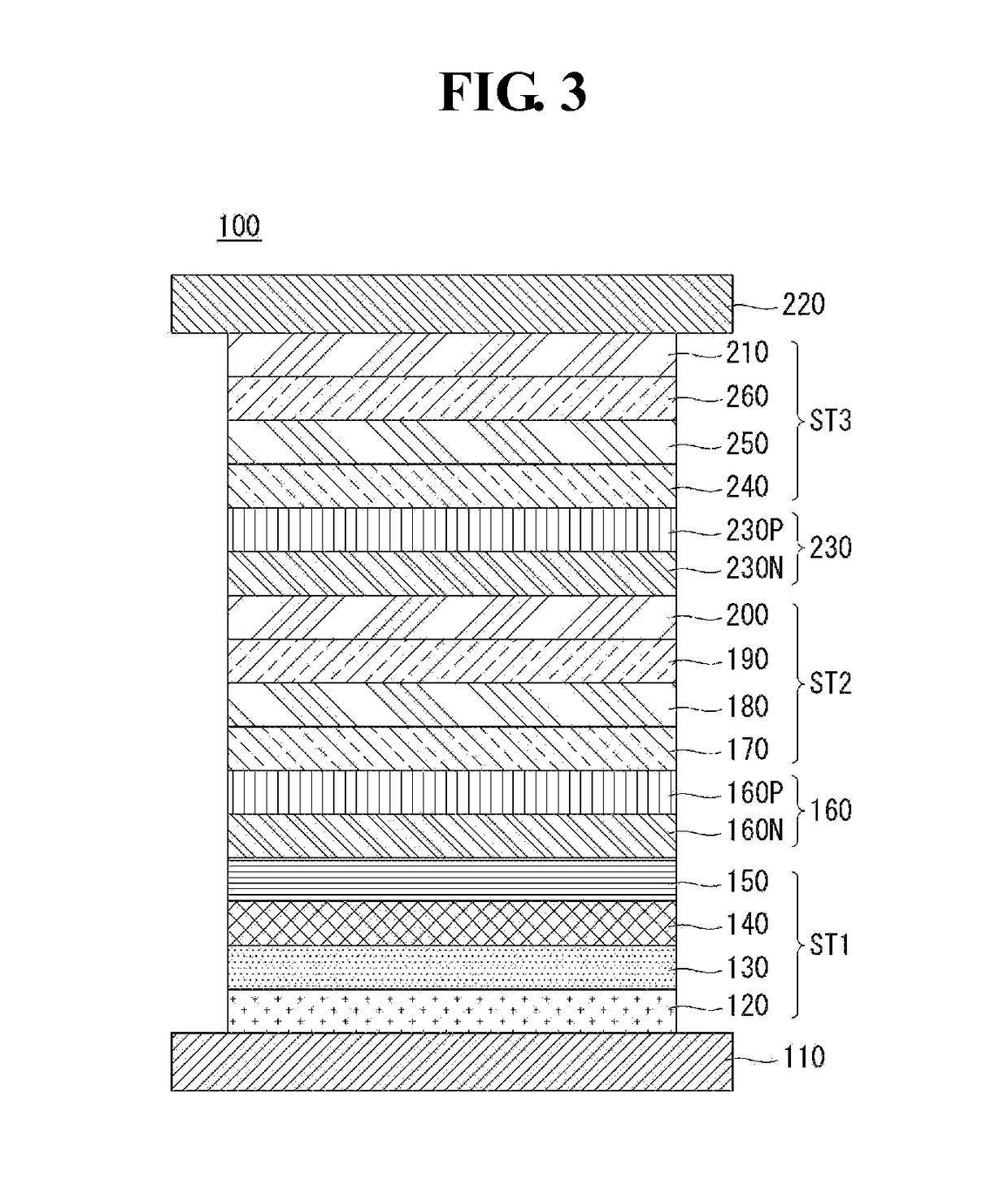
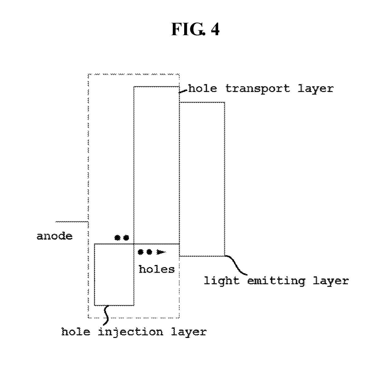
Organic light emitting display device
a light-emitting display and organic technology, applied in the direction of organic semiconductor devices, organic chemistry, nuclear engineering, etc., can solve the problems of thermal stability and deposition stability, affecting the contamination of deposition sources, and difficult to synthesize injecting materials, etc., to achieve the effect of reducing the operating voltag
- Summary
- Abstract
- Description
- Claims
- Application Information
AI Technical Summary
Benefits of technology
Problems solved by technology
Method used
Image

Examples
embodiment 1
[0113]The organic light emitting display device has the same composition as Comparative Example 1, and the hole injection layer was formed with a thickness of 100 Å by doping NPD with the compound A-1 at a 5% doping concentration.
embodiment 2
[0114]The organic light emitting display device has the same composition as Comparative Example 1, and the hole injection layer was formed with a thickness of 100 Å by doping NPD with the compound A-1 at a 10% doping concentration.
[0115]The materials for the hole injection layer used in the above Comparative Examples 1 and 2 and Embodiments 1 and 2 do not limit the scope of the present invention.
[0116]The operating voltage, luminous efficiency, and quantum efficiency of the organic light emitting display devices according to Comparative Examples 1 and 2 and Embodiments 1 and 2 were measured and shown in the following Table 2 (The devices were driven at an operating current of 10 mA / cm2).
[0117]
TABLE 2LuminousOperatingefficiencyQuantumvoltage (V)(Cd / A)efficiency (%)Comparative4.133.84.4Example 1Comparative4.673.84.3Example 2Embodiment 14.033.84.4Embodiment 24.033.84.3
[0118]Referring to Table 2, as compared to Comparative Example 1 using HAT-CN for a hole injection layer, Embodiment 1 ...
PUM
| Property | Measurement | Unit |
|---|---|---|
| thickness | aaaaa | aaaaa |
| thickness | aaaaa | aaaaa |
| thickness | aaaaa | aaaaa |
Abstract
Description
Claims
Application Information