

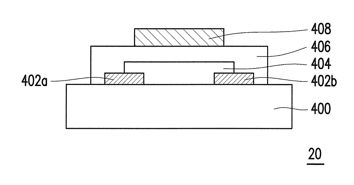
Printed circuit, thin film transistor and manufacturing method thereof
a printed circuit and thin film technology, applied in the direction of printed circuit aspects, conductive pattern formation, semiconductor/solid-state device details, etc., can solve the problems of reducing stability and shortening retention period, reducing stability, and still generating problems, so as to enhance stability and conductivity, increase heat resistance of the circuit, and maintain the effect of conductivity
- Summary
- Abstract
- Description
- Claims
- Application Information
AI Technical Summary
Benefits of technology
Problems solved by technology
Method used
Image

Examples
example 1
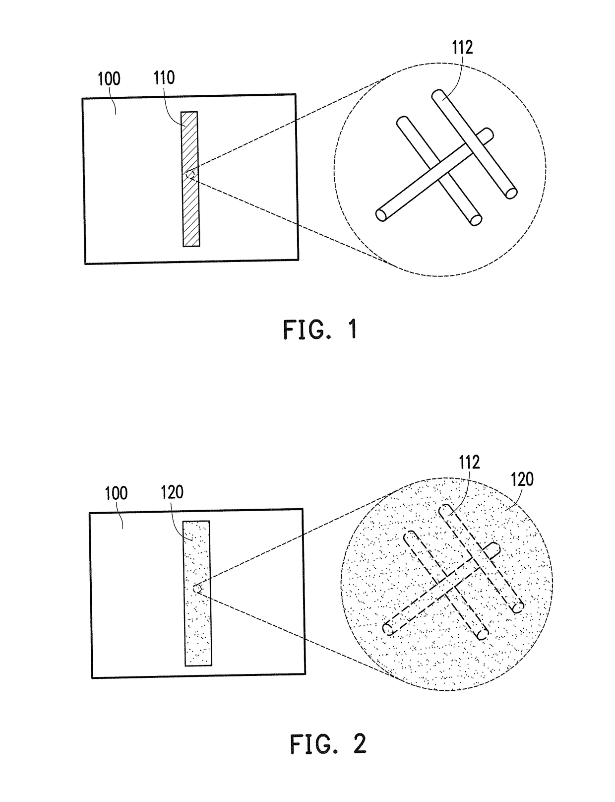
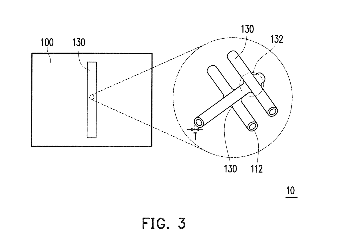
[0039]First, a metal ink containing silver nanowires was printed on a substrate. Next, a colloid composition containing a TiO2 precursor was printed on the metal ink, and then baked at 150° C. for 1 hour to remove a solvent, so that the TiO2 precursor was reduced to TiO2 on the surface of the silver nanowires. At this point, the printed circuit having the TiO2 protective film was formed on the substrate.
[0040]FIG. 5A is an SEM photograph of silver nanowires before printing a colloid composition. FIG. 5B is an SEM photograph of silver nanowires after printing the colloid composition and baking. It can be learned from FIG. 5B that, after the printed colloid composition is baked, the collide is not only formed on the surface of the silver nanowires, but also aggregates at the intersection of the silver nanowires, which helps the bonding between the adjacent silver nanowires, thereby enhancing the stability and the conductivity of the circuit.
[0041][Thermal Stability Test]
example 2
Printing Metal Ink and Colloid Composition Containing TiO2 Precursor
[0042]First, a metal ink containing silver nanowires was printed on a substrate. Next, a colloid composition containing a TiO2 precursor was printed on the metal ink. Then, a heating process was performed to remove a solvent. Then, after baking at 400° C. for 1 hour, the state of the silver nanowires was observed using a scanning electron microscope.
example 3
[0048]First, a metal ink containing silver nanowires was printed on a substrate. Next, a colloid composition containing a TiO2 precursor was printed on the metal ink. Then, a heating process was performed to remove a solvent. Then, after baking at 25° C., 50° C., 100° C., 150° C., 200° C., 250° C., 300° C., and 400° C. for 1 hour respectively, sheet resistance of the silver nanowires having the protective film at each temperature point was measured.
PUM
 Abstract
Description
Claims
Application Information