Semiconductor device having fuse elements

a technology of fuse elements and semiconductors, applied in semiconductor devices, semiconductor/solid-state device details, electrical apparatus, etc., can solve the problems of low mechanical strength of bpsg film and psg film, electrical short circuit between adjacent fuse elements, etc., and achieve the effect of high mechanical strength

Inactive Publication Date: 2018-05-29
ABLIC INC
View PDF13 Cites 0 Cited by
  • Summary
  • Abstract
  • Description
  • Claims
  • Application Information

AI Technical Summary

Benefits of technology

[0023]The present invention has been made to solve the problems described above, and an object of the present invention is to provide a semiconductor device capable of preventing the readhesion of a conductive body from which fuse elements are made, disconnection of the fuse elements, and other troubles when the fuse elements are cut by laser irradiation, despite the narrowness of a space between adjacent fuse elements, while maintaining the moisture resistance of the fuse elements.
[0025]According to the present invention, where the protective insulating film higher in mechanical strength than the second insulating film covers at least the side surfaces of the fuse elements, when one of the fuse elements is irradiated with laser light, the fuse element explodes at the time when a portion of a conductive body of the fuse element that is irradiated with laser light reaches a high vapor pressure level. The force of the explosion is accordingly greater than in the semiconductor device 400 of the related art, thereby blowing the melted and evaporated conductive body far. The resultant effect is that the conductive body has less chance of readhering to the inside of a blow mark formed by the explosion.
[0026]In addition, the presence of the protective insulating film covering the side surfaces of the fuse elements keeps the force of the explosion from spreading in the horizontal direction, thereby preventing the fuse blow mark of the fuse element that is irradiated with laser light from extending to an area above its adjacent fuse element. The exposure of the adjacent fuse element can thus be avoided.

Problems solved by technology

Specifically, the readhesion of the evaporated conductive body causes an electrical short circuit between the adjacent fuse elements 43 that have been cut.
However, while having excellent moisture resistance, a BPSG film and a PSG film are low in mechanical strength.

Method used


Image

  • Semiconductor device having fuse elements
  • Semiconductor device having fuse elements
  • Semiconductor device having fuse elements

Examples


first embodiment

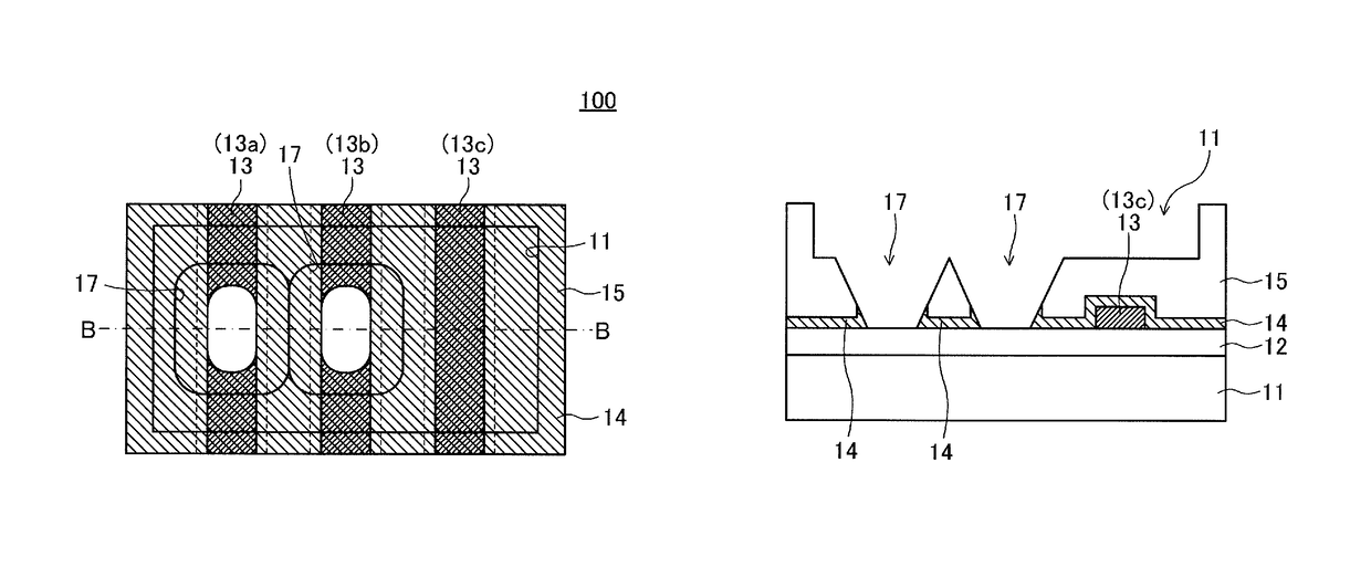
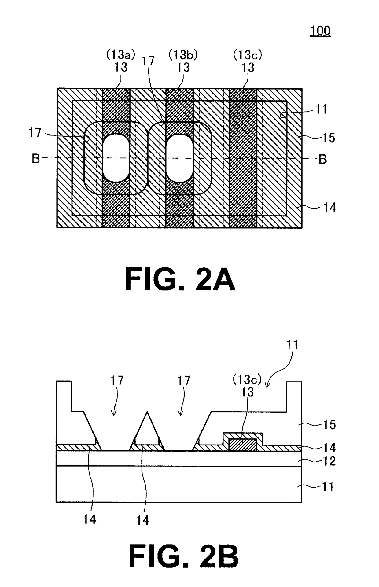
[0037]FIG. 1A and FIG. 1B are diagrams for illustrating the structure of a semiconductor device 100 according to a first embodiment of the present invention. FIG. 1A is a plan view of an area of the semiconductor device 100 that has a plurality of fuse elements formed therein. FIG. 1B is a sectional view taken along the line B-B of FIG. 1A.

[0038]As illustrated in FIG. 1A and FIG. 1B, the semiconductor device 100 of this embodiment includes an insulating film 12 formed on a semiconductor substrate 11, and a plurality of fuse elements 13 (13a, 13b, and 13c) formed on the insulating film 12 from a conductive body, e.g., a polysilicon film and arranged close to one another. A protective insulating film 14 is further formed to cover side surfaces and top surfaces of the plurality of fuse elements 13, and a top surface of the insulating film 12. An insulating film 15 is formed on the protective insulating film 14. A fuse opening 16 for laser irradiation is formed in the insulating film 15...

second embodiment

[0049]FIG. 3A and FIG. 3B are diagrams for illustrating the structure of a semiconductor device 200 according to the second embodiment. FIG. 3A is a plan view of an area of the semiconductor device 200 that has a plurality of fuse elements formed therein. FIG. 3B is a sectional view taken along the line B-B of FIG. 3A.

[0050]In the semiconductor device 200 of this embodiment, a protective insulating film 24 is formed on the left and right side surfaces of each fuse element 13 in place of the protective insulating film 14 in the semiconductor device 100 of the first embodiment which is illustrated in FIG. 1A and FIG. 1B. Similar to the protective insulating film 14, the protective insulating film 24 can be formed of an insulating film that is higher in mechanical strength than the insulating film 15, for example, a silicon nitride film or a silicon oxynitride film.

[0051]The rest of the configuration of the semiconductor device 200 is the same as the semiconductor device 100 of FIG. 1A...

third embodiment

[0059]FIG. 5A and FIG. 5B are diagrams for illustrating the structure of a semiconductor device 300 according to a third embodiment of the present invention. FIG. 5A is a plan view of an area of the semiconductor device 300 that has a plurality of fuse elements formed therein. FIG. 5B is a sectional view taken along the line B-B of FIG. 5A.

[0060]In the semiconductor device 300 of this embodiment, a protective insulating film 34 is formed in place of the protective insulating film 14 in the semiconductor device 100 of the first embodiment which is illustrated in FIG. 1A and FIG. 1B. Similar to the protective insulating film 14, the protective insulating film 34 can be formed of an insulating film that is higher in mechanical strength than the insulating film 15, for example, a silicon nitride film or a silicon oxynitride film.

[0061]The rest of the configuration of the semiconductor device 300 is the same as the semiconductor device 100 of FIG. 1A and FIG. 1B. Components of the semico...


PUM


Abstract

Provided is a semiconductor device preventing readhesion of conductive body which forms fuse elements and breakage of the fuse elements. The semiconductor device includes a first insulating film formed on a semiconductor substrate, a plurality of fuse elements formed on the first insulating film adjacent to one another, a protective insulating film covering at least side surfaces of the fuse elements, and a second insulating film formed of one of a BPSG film and a PSG film to cover the fuse elements and the protective insulating film. The protective insulating film is higher in mechanical strength than the second insulating film.

Description

RELATED APPLICATIONS[0001]This application claims priority under 35 U.S.C. § 119 to Japanese Patent Application No. 2016-017350 filed on Feb. 1, 2016, the entire content of which is hereby incorporated by reference.BACKGROUND OF THE INVENTION[0002]1. Field of the Invention[0003]The present invention relates to a semiconductor device, more particularly, to a semiconductor device having a fuse element which blows by laser irradiation.[0004]2. Description of the Related Art[0005]Fuse elements are generally and widely used in adjustment of a resistance value of a semiconductor device or fixing a setting of a redundant circuit. Cutting of a fuse element gives a change from a conductive state to a non-conductive state occurs, and desired information is stored in a trimming circuit. Cutting of a fuse element is done by a method of making a fuse element blow by laser irradiation, a method of making a fuse element melt and separate by a flow of a large current, or the like.[0006]A fuse eleme...

Claims


Application Information

Patent Timeline
Patent Type & Authority Patents(United States)
IPC IPC(8): H01L23/52H01L23/62H01L23/532H01L23/525
CPCH01L23/5258H01L23/53209H01L23/53257H01L23/53295H01L23/53271H01L23/62H01L23/5256H01L2924/0002H01L2924/00H01L23/522H01L21/0217H01L21/3211
Inventor KIMURA, YOSHITAKA
Owner ABLIC INC
Why Eureka
Try Eureka