Light-emitting element having a delayed fluorescence component due to triplet-triplet annihilation

a technology of triplet-triplet and light-emitting elements, which is applied in the direction of static indicating devices, instruments, solid-state devices, etc., can solve the problems that the light-emitting element that emits blue light has not been put into practical use, and achieve the effect of improving the emission efficiency increasing the proportion of the delayed fluorescence component due to tta in the emissive components of the light-emitting elemen

Active Publication Date: 2018-05-29
SEMICON ENERGY LAB CO LTD
View PDF108 Cites 3 Cited by
  • Summary
  • Abstract
  • Description
  • Claims
  • Application Information

AI Technical Summary

Benefits of technology

[0013]What is essential to improve the emission efficiency of a light-emitting element including a fluorescent material is that the energy of triplet excitons, which do not contribute to light emission, is converted into the energy of singlet excitons with light-emitting properties and the conversion efficiency is increased. In other words, it is important to convert the energy of triplet excitons into the energy of singlet excitons by TTA; in particular, the proportion of a delayed fluorescence component due to TTA in the emissive components of the light-emitting element should be increased. This is because an increased proportion of the delayed fluorescence component due to TTA means an increase in the production rate of singlet excitons with light-emitting properties.
[0014]In view of the above, an object of one embodiment of the present invention is to provide a light-emitting element that includes a fluorescent material and has a high emission efficiency. Another object of one embodiment of the present invention is to provide a light-emitting element in which a delayed fluorescence component due to TTA accounts for a high proportion of emissive components. Another object of one embodiment of the present invention is to provide a novel light-emitting device with a high emission efficiency and a low power consumption. Another object of one embodiment of the present invention is to provide a novel display device.
[0022]According to one embodiment of the present invention, a light-emitting element that includes a fluorescent material and has a high emission efficiency can be provided. According to another embodiment of the present invention, a light-emitting element in which a delayed fluorescence component due to TTA accounts for a high proportion of emissive components can be provided. According to another embodiment of the present invention, a novel light-emitting device with a high emission efficiency and a low power consumption can be provided. According to another embodiment of the present invention, a novel display device can be provided.

Problems solved by technology

Among the light-emitting elements including phosphorescent materials, a light-emitting element that emits blue light has not been put into practical use yet because it is difficult to develop a stable material having a high triplet excitation energy level.

Method used


Image

  • Light-emitting element having a delayed fluorescence component due to triplet-triplet annihilation
  • Light-emitting element having a delayed fluorescence component due to triplet-triplet annihilation
  • Light-emitting element having a delayed fluorescence component due to triplet-triplet annihilation

Examples


embodiment 1

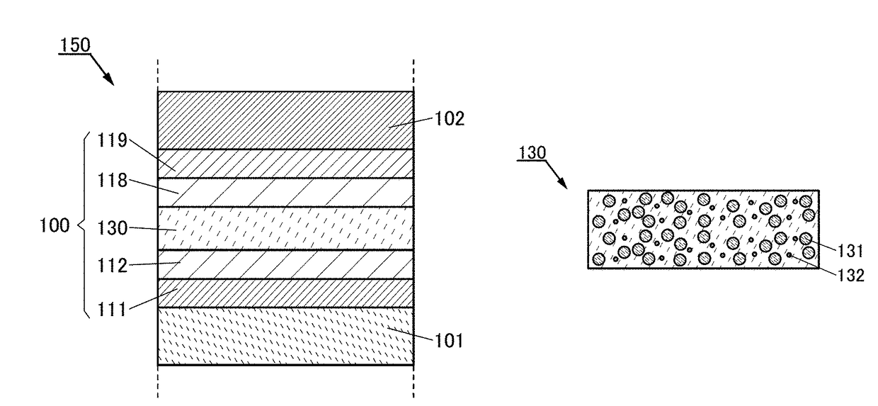
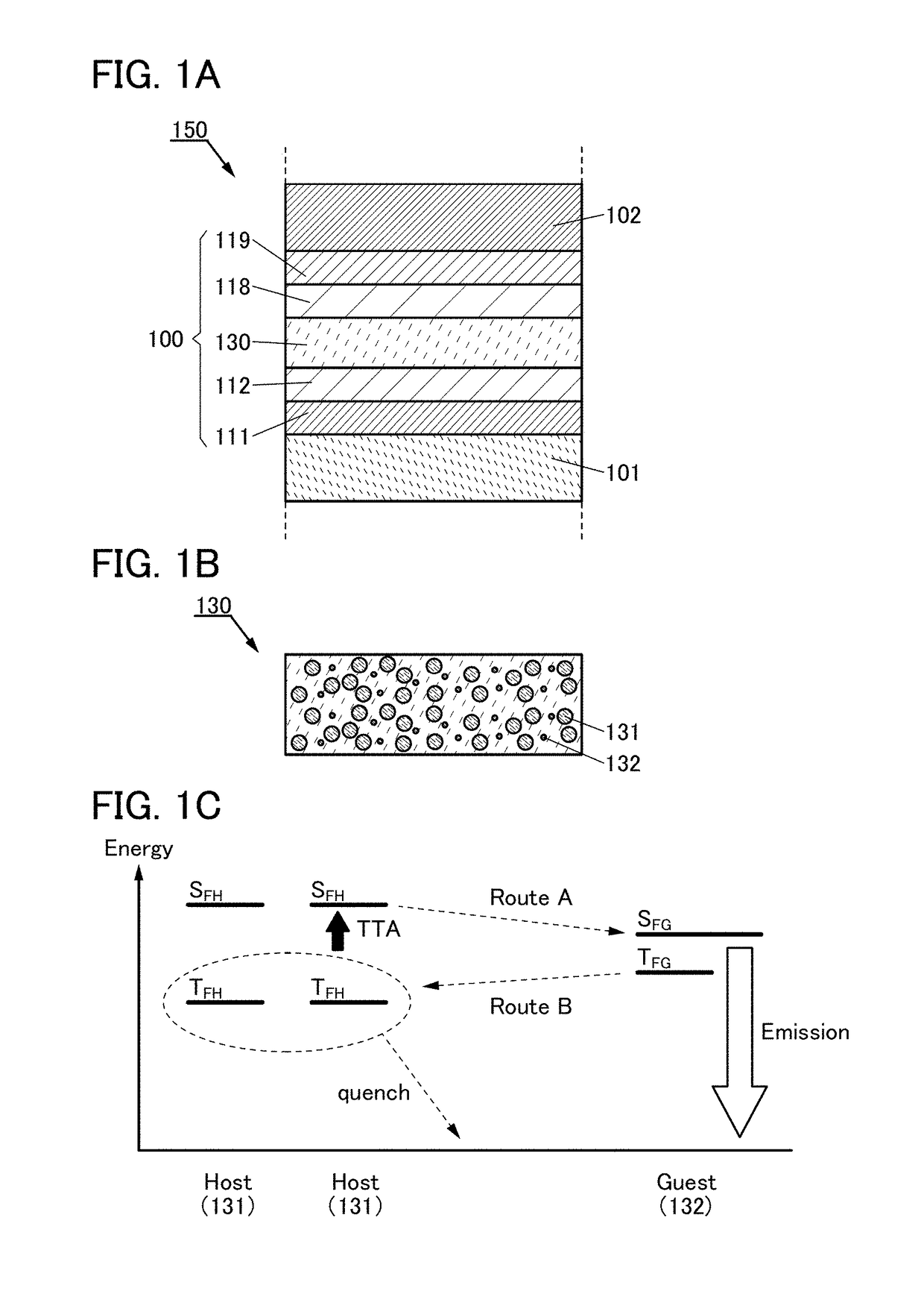
[0065]First, a structure of a light-emitting element of one embodiment of the present invention will be described below with reference to FIGS. 1A to 1C.

[0066]FIG. 1A is a schematic cross-sectional view of a light-emitting element 150 of one embodiment of the present invention.

[0067]The light-emitting element 150 includes a pair of electrodes (an electrode 101 and an electrode 102) and an EL layer 100 therebetween. The EL layer 100 includes at least a light-emitting layer 130. Note that the description in this embodiment is given assuming that the electrode 101 and the electrode 102 of the pair of electrodes serve as an anode and a cathode, respectively; however, they can be interchanged for the structure of the light-emitting element 150.

[0068]The EL layer 100 illustrated in FIG. 1A includes functional layers in addition to the light-emitting layer 130. The functional layers include a hole-injection layer 111, a hole-transport layer 112, an electron-transport layer 118, and an elec...

embodiment 2

[0181]In this embodiment, structure examples of the light-emitting element of one embodiment of the present invention, which is described in Embodiment 1, will be described with reference to FIG. 5 to FIG. 7B.

[0182]A structure example of the light-emitting element of one embodiment of the present invention will be described below with reference to FIG. 5. FIG. 5 is a cross-sectional view illustrating a light-emitting element of one embodiment of the present invention.

[0183]A light-emitting element 250 in FIG. 5 has a bottom-emission structure in which light is extracted through a substrate 200. However, one embodiment of the present invention is not limited to this structure and may have a top-emission structure in which light emitted from the light-emitting element is extracted in the direction opposite to the substrate 200 or a dual-emission structure in which light emitted from the light-emitting element is extracted in both top and bottom directions of the substrate 200 over whi...

embodiment 3

[0211]In this embodiment, light-emitting elements having structures different from those described in Embodiments 1 and 2 and emission mechanisms of the light-emitting elements will be described below with reference to FIG. 7A to FIG. 8B.

[0212]FIG. 7A is a schematic cross-sectional view of a light-emitting element 450.

[0213]The light-emitting element 450 illustrated in FIG. 7A includes a plurality of light-emitting units (a light-emitting unit 441 and a light-emitting unit 442 in FIG. 7A) between a pair of electrodes (an electrode 401 and an electrode 402). One light-emitting unit has the same structure as the EL layer 100 illustrated in FIG. 1A. That is, the light-emitting element 150 in FIG. 1A includes one light-emitting unit, whereas the light-emitting element 450 includes a plurality of light-emitting units. Note that the electrode 401 functions as an anode and the electrode 402 functions as a cathode in the following description of the light-emitting element 450; however, the ...


PUM


Abstract

A light-emitting element that includes a fluorescent material and has a high emission efficiency is provided. A light-emitting element in which a delayed fluorescence component due to TTA accounts for a high proportion of emissive components is provided. A novel light-emitting device with a high emission efficiency and a low power consumption is provided. A light-emitting element includes an anode, a cathode, and an EL layer. The EL layer includes a light-emitting layer including a host material and an electron-transport layer including a first material in contact with the light-emitting layer. The LUMO level of the first material is lower than that of the host material. The proportion of a delayed fluorescence component due to TTA is greater than or equal to 10 percent of the light emission from the EL layer. The proportion of the delayed fluorescence component due to TTA may be greater than or equal to 15 percent of the light emission.

Description

TECHNICAL FIELD[0001]One embodiment of the present invention relates to a light-emitting element, a display module, a lighting module, a display device, a light-emitting device, an electronic device, and a lighting device. Note that one embodiment of the present invention is not limited to the above technical field. The technical field of one embodiment of the invention disclosed in this specification and the like relates to an object, a method, or a manufacturing method. Furthermore, one embodiment of the present invention relates to a process, a machine, manufacture, or a composition of matter. In particular, examples of the technical field of one embodiment of the present invention disclosed in this specification include a semiconductor device, a display device, a liquid crystal display device, a light-emitting device, a lighting device, a power storage device, a memory device, an imaging device, a method for driving any of them, and a method for manufacturing any of them.BACKGRO...

Claims


Application Information

Patent Timeline
Patent Type & Authority Patents(United States)
IPC IPC(8): H01L51/50H01L51/00
CPCH01L51/5016H01L51/5056H01L51/5072H01L51/006H01L51/0074H01L51/0054H01L51/0058H01L51/0067H01L51/0072H01L51/0052H10K50/11H10K2101/40H10K50/16H10K2101/30H10K59/38H10K59/40H10K85/633H10K85/654H10K85/6576H10K85/6572H10K50/865H10K85/622H10K85/626H10K85/615H10K50/15G09G2300/0804G09G3/3266H01L27/14678G09G3/3275G09G2300/0408H10K50/14H10K50/17H10K50/171H10K50/818H10K50/856H10K50/8426H10K59/32H10K59/35H10K59/126H10K59/131H10K59/1216H10K2101/10H10K2101/90
Inventor HASHIMOTO, NAOAKISUZUKI, TSUNENORISEO, SATOSHISEO, HIROMIKIDO, HIROMITSU
Owner SEMICON ENERGY LAB CO LTD
Why Eureka
Try Eureka