Program circuit

Inactive Publication Date: 2008-02-19
DOSILICON CO LTD
View PDF8 Cites 0 Cited by
  • Summary
  • Abstract
  • Description
  • Claims
  • Application Information

AI Technical Summary

Benefits of technology

[0007]It is therefore an object of the present invention to provide a program circuit which can apply a program bias voltage only to the memory cell which is not programmed during a re-programming operation.

Problems solved by technology

In a conventional flash memory device, however, a program bias voltage is applied to a memory cell which is already programmed during a re-programming operation, thus the already programmed memory cell is damaged.
As a result, reliability of the memory cell is degraded.

Method used


Image

  • Program circuit
  • Program circuit

Examples


Embodiment Construction

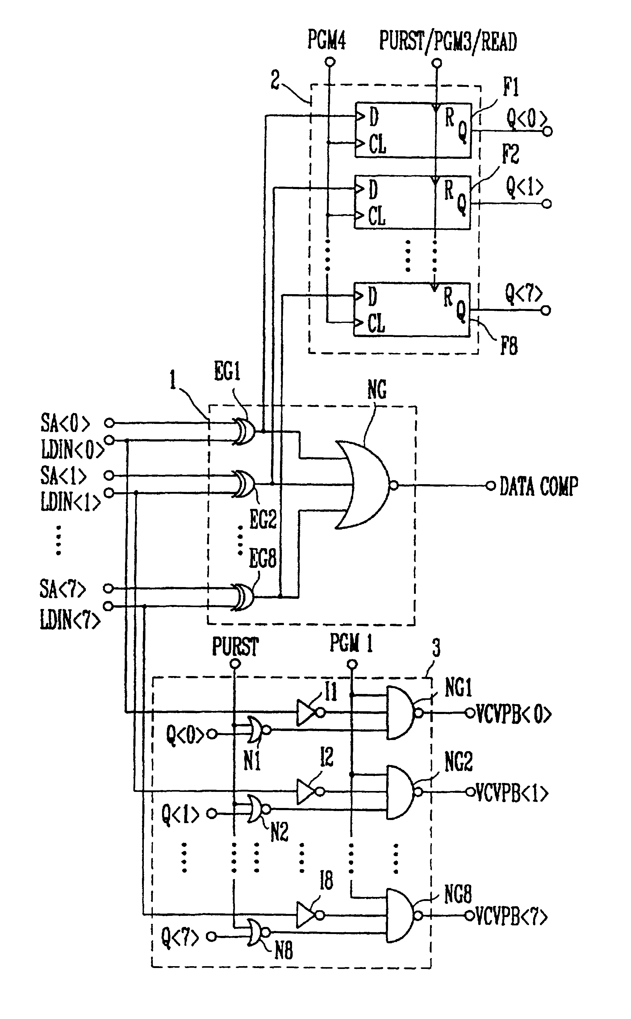
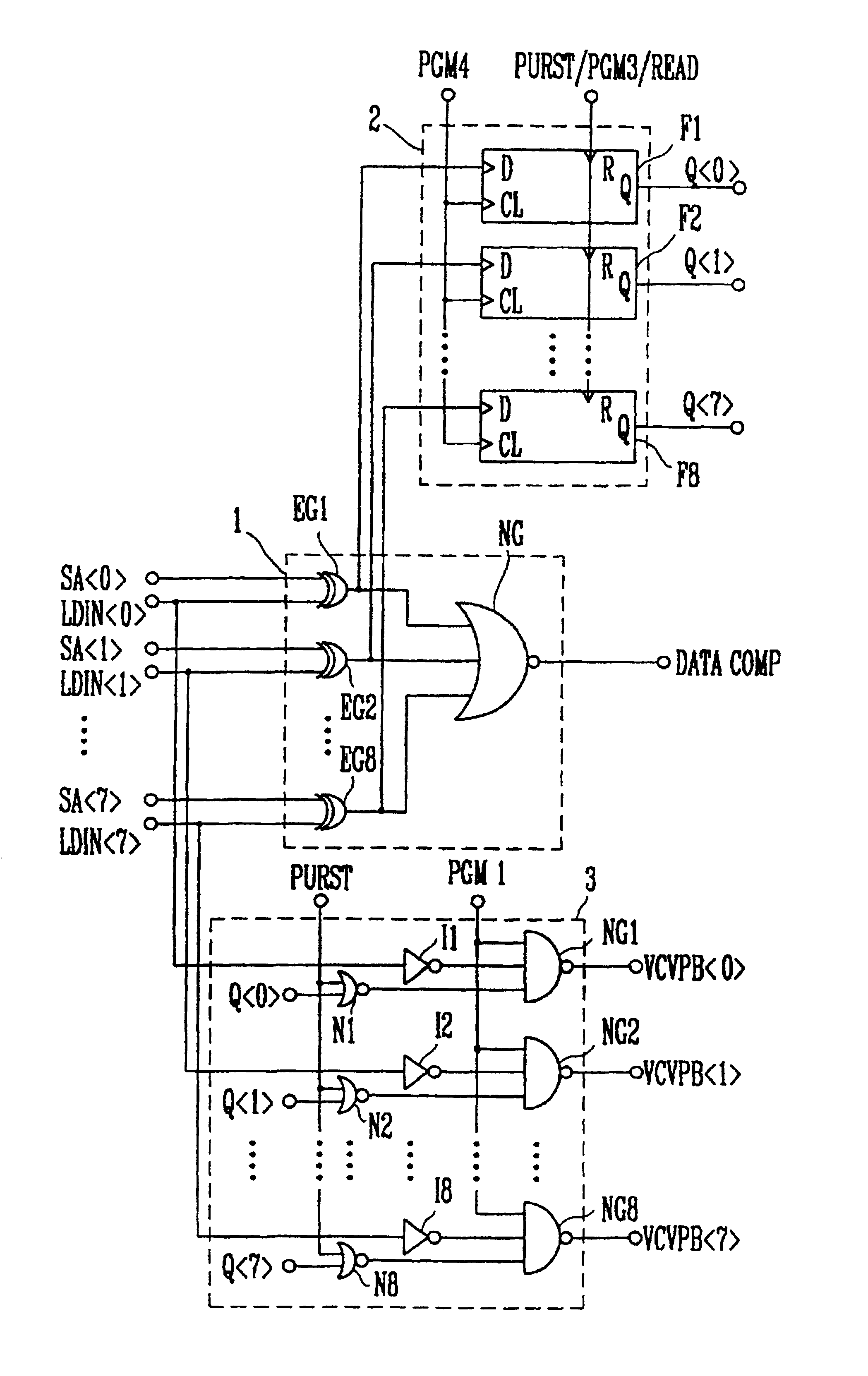
[0014]The accompanying drawing is a circuit diagram for explaining a program circuit according to the present invention.

[0015]The program circuit according to the present invention is consisted of a comparator 1, a data latch circuit 2, and a control circuit for generating a high voltage 3, and added to the flash memory device.

[0016]The comparator 1 comprises of a plurality of exclusive NOR gates EG1 through EG8 to which output data LDIN0 through LDIN7 of a data input buffer and output data SA0 through SA7 of a sense amplifier are inputted, respectively. Also, the comparator 1 comprises a NOR gate NG to which output signals of the exclusive NOR gates EG1 through EG8 are inputted. The NOR gate NG outputs logical combination signals via an output terminal DATA COMP.

[0017]The data latch circuit 2 is consisted of a plurality of flip-flops F1 through F8. Each of flip-flops F1 through F8 comprises a data input terminal D to which an output signal of one of the exclusive NOR gates EG1 thro...


PUM


Abstract

The program circuit according to the present invention can apply a program voltage to the only memory cells which are not programmed during a re-programming operation, thus, the present invention can be prevent a lowering of reliability of the memory cell due to a continued supply of a program bias voltage.

Description

[0001]This application is a Reissue application of U.S. patent application Ser. No. 08 / 882,835, filed on Jun. 26, 1997, now U.S. Pat. No. 5,930,179.BACKGROUND OF THE INVENTION[0002]1. Field of the Invention[0003]The present invention relates to a program circuit and, more particularly, to a program circuit which can prevent a lowering of reliability occurring during the process of verifying the programmed data.[0004]2. Description of the Prior Arts[0005]Generally, a flash memory device has functions of electrical program and erasure. The flash memory device also performs a verification operation so as to confirm whether the memory cell has been programmed or erased or not after completion of the programming or the erasure operation. At this time, if there are memory cells in which a programming or erasure operation has not completed, re-programming or re-erasure operation is performed again.[0006]In a conventional flash memory device, however, a program bias voltage is applied to a ...

Claims


Application Information

Patent Timeline
IPC IPC(8): G11C16/34G11C16/10
CPCG11C16/10G11C16/3459G11C16/3468G11C16/3486G11C16/3418G11C16/26G11C16/30G11C7/1087
Inventor CHA, BYOUNG KWON
Owner DOSILICON CO LTD
Why Eureka
Try Eureka