Method of forming pre-metal dielectric film on a semiconductor substrate including first layer of undoped oxide of high ozone:TEOS volume ratio and second layer of low ozone doped BPSG

a dielectric film and semiconductor substrate technology, applied in the field of semiconductor processing, can solve problems such as void-free dielectric film surface, achieve good gettering capability, good as-deposited gapfill characteristics, and sacrifice good mobile-ion gettering properties

Inactive Publication Date: 2008-09-16
SAMSUNG ELECTRONICS CO LTD
View PDF19 Cites 0 Cited by
  • Summary
  • Abstract
  • Description
  • Claims
  • Application Information

AI Technical Summary

Benefits of technology

[0010]The above objects have been achieved by a method of forming a pre-metal dielectric film having good as-deposited gapfill characteristics, as well as good gettering capability. The method involves first depositing a layer of high-ozone undoped silicon dioxide film that provides the void-free gapfill characteristic and then depositing a low-ozone doped BPSG film that provides the gettering capability. This two layer insulating film provides the ability to have the gaps adequately filled between small or narrow lines without sacrificing good mobile-ion gettering properties. Prior art insulating films tend to provide either good gapfill or good gettering but not both, or the prior art films require several layers to achieve the desired properties.
[0011]The undoped silicon dioxide film has a high ozone / TEOS volume ratio of at least 15 to 1, as compared to the prior art doped BPSG film which generally have lower ozone / TEOS ratios, such as 10 to 1. By forming a film with a high ozone / TEOS ratio, the surface mobility of the TEOS-dimer is increased, causing the film to have better flow characteristics. The reactants can diffuse readily on the surface, thus finding the regions having the lowest energy. This results in a void-free dielectric film surface.
[0012]A heat treatment is then applied to densify the film, rather than to soften and flow the film as is done in the prior art. This allows the best treatment to be conducted at a lower temperature, which prevents the diffusion problems described above that are associated with high temperature heat treatment in smaller device geometries. Finally, the top of the second BPSG layer is planarized using chemical mechanical planarization. The method of the present invention can be used in the formation of semiconductor devices and can be also used in the formation of other structures requiring a good gapfill or step coverage, such as the formation of polysilicon bus structures.

Problems solved by technology

This results in a void-free dielectric film surface.

Method used


Image

  • Method of forming pre-metal dielectric film on a semiconductor substrate including first layer of undoped oxide of high ozone:TEOS volume ratio and second layer of low ozone doped BPSG
  • Method of forming pre-metal dielectric film on a semiconductor substrate including first layer of undoped oxide of high ozone:TEOS volume ratio and second layer of low ozone doped BPSG
  • Method of forming pre-metal dielectric film on a semiconductor substrate including first layer of undoped oxide of high ozone:TEOS volume ratio and second layer of low ozone doped BPSG

Examples


Embodiment Construction

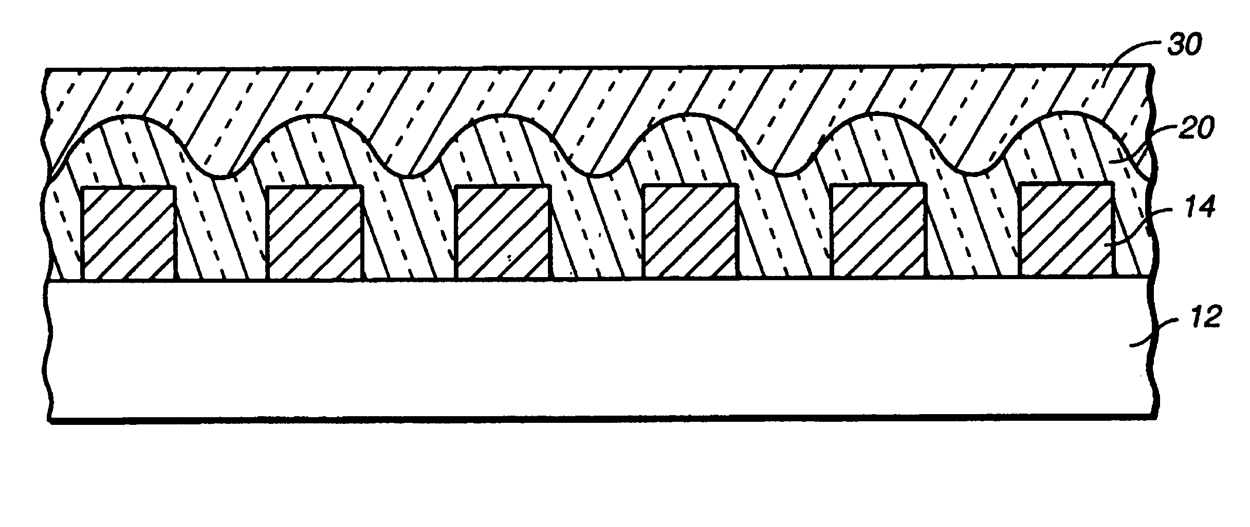
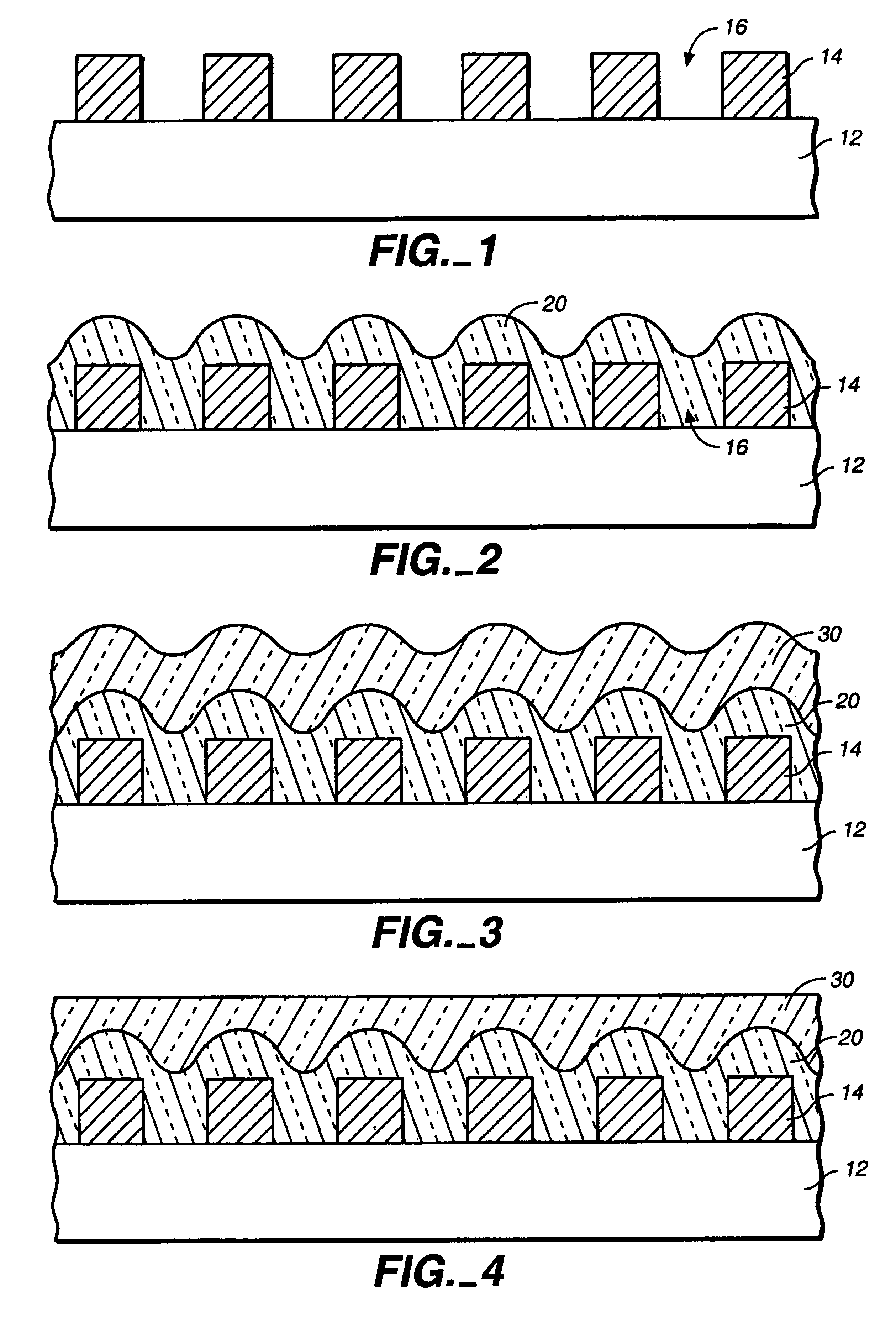
[0016]With reference to FIG. 1, a silicon substrate 12 has a plurality of polysilicon conductors 14 formed on a top surface thereof. It is understood that the silicon substrate 12 has undergone the various steps of wafer preparation previous to the method of the present invention in order to form the various diodes, transistors, and resistors and other components on the substrate. This is done by adding dopants to the pure silicon in a manner that is well known in the art. The polysilicon conductors 14 are also formed on the top surface of the substrate in a manner that is known in the art. Between each of the polysilicon conductors 14 are gaps 16 which will need to be filled with electrically isolating dielectric film.

[0017]With reference to FIG. 2, a layer of high ozone undoped silicon dioxide film 20 is deposited on top of the semiconductor substrate 12 and the polysilicon conductors 14. The high ozone undoped silicon dioxide film covers the polysilicon conductors 14 and fills th...


PUM

PropertyMeasurementUnit
volume ratioaaaaaaaaaa
thicknessaaaaaaaaaa
thicknessaaaaaaaaaa

Abstract

A method of forming a pre-metal dielectric film having good as deposited gapfill characteristics, as well as good mobile-ion gettering capability. The method involves first depositing a layer of high-ozone undoped silicon dioxide film having a high ozone/TEOS volume ratio. Then, a low-ozone doped BPSG film is deposited over the high-ozone undoped silicon dioxide layer. The film layers are heat treated to densify the film, and then the top layer is planarized using known planarization techniques to a thickness that allows for adequate mobile-ion gettering.

Description

TECHNICAL FIELD[0001]This invention relates to semiconductor processing and, more particularly, to a method of forming a dielectric film on a semiconductor substrate and to a method of forming a semiconductor device having this dielectric film.BACKGROUND ART[0002]In the formation of semiconductor integrated circuit devices, a frequent practice in the planar process is to form subsurface diffusion layers and polysilicon conductors on a silicon substrate surface. One or more dielectric films are deposited over the silicon substrate surface and metal wiring conductors are formed on or in the dielectric film to interconnect the various components formed on the silicon substrate surface to achieve the desired integrated circuit.[0003]It is desirable that the dielectric films which are deposited on the substrate prior to the metallization process have a good mobile-ion gettering property, as well as a good reflow or gapfill property. A type of insulating film that has been widely used in ...

Claims


Application Information

Patent Timeline
Patent Type & Authority Patents(United States)
IPC IPC(8): H01L21/31H01L21/469C23C16/42H01L21/3105H01L21/316
CPCH01L21/02129H01L21/02164H01L21/022H01L21/02271H01L21/31051H01L21/324H01L21/31612H01L21/31625
Inventor KELKAR, AMIT S.WHITEMAN, MICHAEL D.
Owner SAMSUNG ELECTRONICS CO LTD
Why Eureka
Try Eureka