Semiconductor device having an improved connected arrangement between a semiconductor pellet and base substrate electrodes

a technology of semiconductor pellets and electrodes, which is applied in the direction of semiconductor devices, semiconductor/solid-state device details, coatings, etc., can solve the problems of reducing the operating speed of the semiconductor device, increasing the size of the semiconductor device as a whole, and increasing the inductance, so as to increase the connection strength between the bonding wires and the second electrode pads. , the effect of increasing the young's modulus

Inactive Publication Date: 2010-09-21
RENESAS TECH CORP
View PDF53 Cites 58 Cited by
  • Summary
  • Abstract
  • Description
  • Claims
  • Application Information

AI Technical Summary

Benefits of technology

[0014]The circuit systems formed on the typical semiconductor pellets 2 have tended to grow in their level of integration and the number of functions they perform. With enhanced integration and more diversified functions of the circuit system, the number of bonding pads 2A of the semiconductor pellet 2 and the number of second electrode pads 1A of the base substrate 1 increase. That is, the number of through-hole conductors 1C electrically connecting the second electrode pads 1A and the first electrode pads 1B increases as the integration and function of the circuit system are enhanced. Hence, there has been a problem that the external size of the base substrate 1 increase with the increasing number of the through-hole conductors 1C, which in turn increases the size of the semiconductor device as a whole.
[0034]Furthermore, the base substrate used is formed of a rigid substrate having a small planar thermal expansion coefficient and a high Young's modulus compared with those of a flexible substrate, which means the rigid substrate is harder to bend. As a result, the rigid base substrate is free from deformations (warping or twisting) due to reflow heat during the process of mounting the semiconductor device on the mounting surface of the mounting board. As a result, a sufficient degree of flatness of the back of the base substrate with respect to the mounting surface of the mounting board can be secured, which in turn allows the manufacture of semiconductor devices with high mounting precision.

Problems solved by technology

Hence, there has been a problem that the external size of the base substrate 1 increase with the increasing number of the through-hole conductors 1C, which in turn increases the size of the semiconductor device as a whole.
There is also another problem which the inventors have considered.
This, in turn, increases inductance and reduces the operating speed of the semiconductor device.
This gives rise to an apprehension that the connection strength between the bonding wires and the second electrode pads may decrease, leading to connection failures of bonding wires and reduced electric reliability of the semiconductor device.

Method used


Image

  • Semiconductor device having an improved connected arrangement between a semiconductor pellet and base substrate electrodes
  • Semiconductor device having an improved connected arrangement between a semiconductor pellet and base substrate electrodes
  • Semiconductor device having an improved connected arrangement between a semiconductor pellet and base substrate electrodes

Examples


embodiment 1

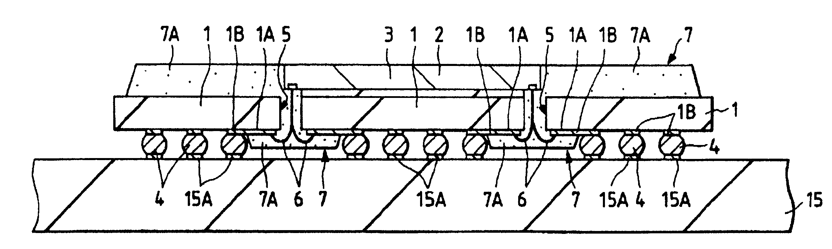
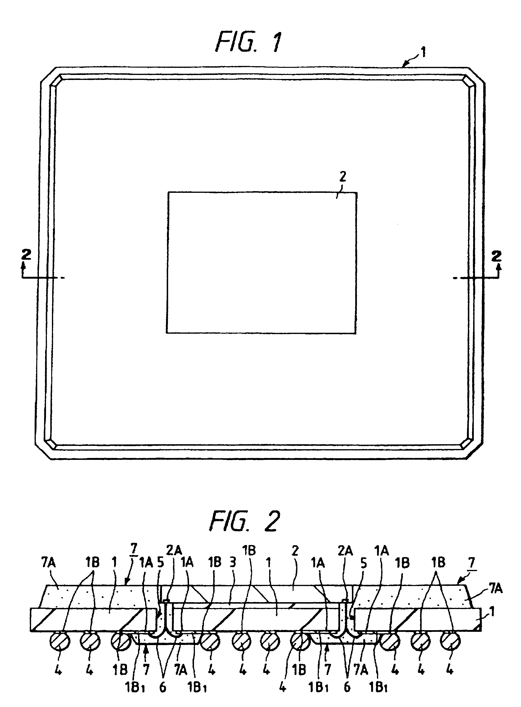
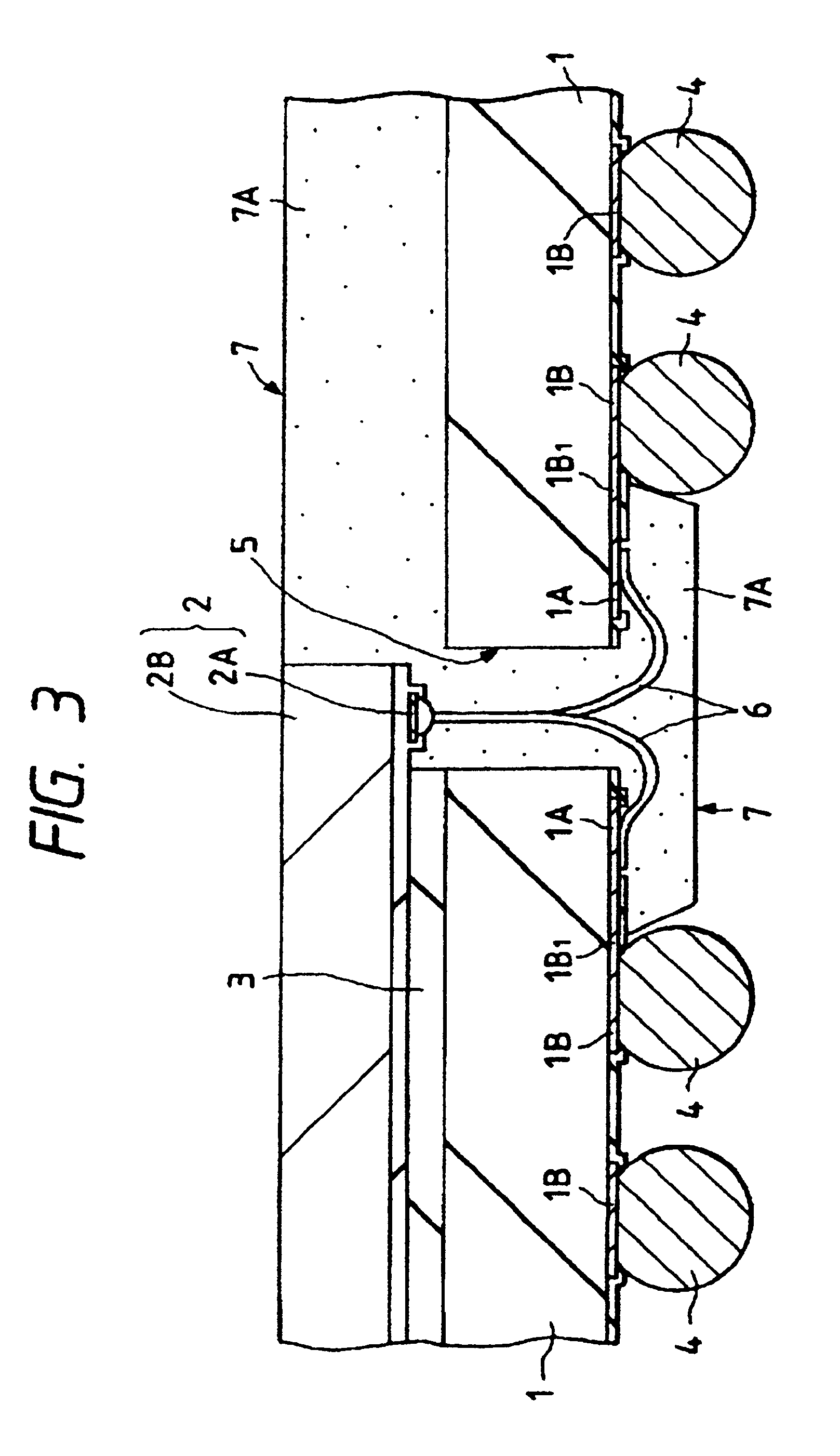
[0052]The outline construction of a semiconductor device, as a first embodiment of this invention, that uses the BGA structure is shown in FIG. 1 (plan view of the main surface side), FIG. 2 (cross section taken along the line A—A of FIG. 1), FIG. 3 (enlarged cross section of an essential part of FIG. 2) and FIG. 4 (enlarged plan view showing the back side of an essential part of the semiconductor device with the resin sealing body removed).

[0053]As shown in FIGS. 1, 2, 3 and 4, the semiconductor device has a semiconductor pellet 2 mounted on a pellet mounting area of the main surface of a base substrate 1, with a plurality of bump electrodes 4 arranged in grid on the back of the base substrate 1 opposite the main surface.

[0054]The base substrate 1 may be formed of a printed circuit board. The printed circuit board may, for example, have a structure in which wiring is formed over the surface of a rigid substrate of glass fiber impregnated with epoxy resin, polyimide resin or maleimi...

embodiment 2

[0104]The outline configuration of a semiconductor device as the second embodiment of this invention that employs a BGA structure is shown in FIG. 12 (cross section) and FIG. 13 (enlarged plan view of an essential part of the back side showing the state of the back side removed of the resin sealing body).

[0105]As shown in FIG. 12 and 13, the semiconductor device has the semiconductor pellet 2 mounted facedown on the pellet mounting area of the main surface of the base substrate 1 with an insulating layer 3 in between. A plurality of bump electrodes 4 are arranged in grid on the back of the base substrate 1.

[0106]Arranged in the central area of the main surface of the semiconductor pellet 2 along the longer sides thereof is a row of bonding pads 2A, which are electrically connected to the second electrode pads 1A arranged on the back of the base substrate 1 through the bonding wires 6 passing through the slits 5 formed in the base substrate 1. The second electrode pads 1A are electri...

embodiment 3

[0109]The outline configuration of a semiconductor device as the third embodiment of this invention that employs a BGA structure is shown in FIG. 14 (plan view of an essential part of the back side showing the state of the back side removed of the resin sealing body).

[0110]As shown in FIG. 14, the semiconductor device has a semiconductor pellet 2 mounted facedown on a pellet mounting area of the main surface of the base substrate 1, with an insulating layer 3 in between. Bump electrodes 4 are arranged in grid on the back of the base substrate 1.

[0111]At the outer periphery of the main surface of the semiconductor pellet 2, a plurality of bonding pads 2A are arranged along the sides of the pellet. At the central portion of the main surface of the semiconductor pellet 2, a plurality of bonding pads 2A are arranged along the longer or shorter side of the pellet. The bonding pads 2A are electrically connected to the second electrode pads 1A arranged on the back of the base substrate 1 b...


PUM

PropertyMeasurementUnit
outer diameteraaaaaaaaaa
Young's modulusaaaaaaaaaa

Abstract

A semiconductor device comprising a semiconductor pellet mounted on a pellet mounting area of the main surface of a base substrate, in which first electrode pads arranged on the back of the base substrate are electrically connected to bonding pads arranged on the main surface of the semiconductor pellet. The base substrate is formed of a rigid substrate, and its first electrode pads are electrically connected to the second electrode pads arranged on its reverse side. The semiconductor pellet is mounted on the pellet mounting area of the main surface of the base substrate, with its main surface downward, and its bonding pads are connected electrically with the second electrode pads of the base substrate through bonding wires passing through slits formed in the base substrate.

Description

[0001]More than one reissue application has been filed for the reissue of U.S. Pat. No. 5,777,391. These reissue applications are the present application Ser. No. 09 / 613,541, filed Jul. 7, 2000; Ser. No. 10 / 105,236, filed on Mar. 26, 2002; Ser. No. 11 / 182,039 filed on Jul. 15, 2005; Ser. No. 11 / 182,040, also filed on Jul. 15, 2005; Ser. No. 11 / 256,620, filed on Oct. 24, 2005; Ser. No. 11 / 256,621, also filed on Oct. 24, 2005; Ser. No. 11 / 285,730, filed on Nov. 23, 2005 and Ser. No. 11 / 285,729, filed on Nov. 23, 2005.[0002]The present reissue application also claims the benefit under 35 USC §120 of the filing date of Dec. 11, 1995 of Ser. No. 08 / 570,646, now U.S. Pat. No. 5,777,391, and benefit under 35 USC §119 of Japanese Application No. 6-316,444, filed on Dec. 20, 1994 and Japanese Application No. 7-126405, filed May 25, 1995, the subject matter of which is incorporated herein by reference. <?insert-end id="INS-S-00001" ?>BACKGROUND OF THE INVENTION[0003]The present inventio...

Claims


Application Information

Patent Timeline
Patent Type & Authority Patents(United States)
IPC IPC(8): H01L23/13H01L23/28H01L23/14H01L23/31H01L23/48H01L23/12H01L23/498H01L25/10H01L21/60
CPCB29C45/14655H01L23/13H01L23/3128H01L23/49816H01L23/49827H01L24/05H01L24/06H01L24/32H01L24/48H01L24/49B29C45/0046B29C45/14836H01L24/29H01L24/45H01L2224/0401H01L2224/04042H01L2224/05556H01L2224/06135H01L2224/06136H01L2224/16H01L2224/32014H01L2224/32225H01L2224/45124H01L2224/45144H01L2224/45147H01L2224/45565H01L2224/4569H01L2224/48091H01L2224/48221H01L2224/48227H01L2224/48235H01L2224/4824H01L2224/48465H01L2224/48599H01L2224/48699H01L2224/49175H01L2224/73215H01L2224/73265H01L2224/85206H01L2224/85207H01L2224/92247H01L2924/01004H01L2924/01006H01L2924/01013H01L2924/01014H01L2924/01029H01L2924/0105H01L2924/01079H01L2924/01082H01L2924/15311H01L2924/18161H01L2924/18165H01L2924/30107H01L2924/01005H01L2924/01023H01L2924/01033H01L2924/01075H01L2924/0132H01L2924/1579H01L2224/29111H01L2224/2919H01L2224/48799H01L2224/05554H01L2924/00014H01L2924/00H01L2224/13111H01L2924/0695H01L2924/00012H01L2924/0665H01L2924/351H01L2924/181H01L24/73H01L2224/85399H01L2224/05599H01L21/60
Inventor NAKAMURA, ATSUSHINISHI, KUNIHIKO
Owner RENESAS TECH CORP
Why Eureka
Try Eureka