LCD and method of improving the brilliance of the same

Inactive Publication Date: 2011-04-12
CHUNGHWA PICTURE TUBES LTD
View PDF14 Cites 0 Cited by
  • Summary
  • Abstract
  • Description
  • Claims
  • Application Information

AI Technical Summary

Benefits of technology

[0008]It is the main object of the present invention to provide a liquid crystal display device to eliminate alignment error from the photo-exposure of lithographic process and the alignment errors of overlapped area between drains and gates in different exposure areas, to prevent the phenomenon of shot mura and to improve the uniformity of display panel brilliance.
[0009]It is another object of the present invention to provide a method for manufacturing a liquid crystal display device, to eliminate alignment error from the photo-exposure of lithographic process and the alignment errors of overlapped area between drains and gates in different exposure areas, to prevent the phenomenon of shot mura and to improve the uniformity of display panel brilliance, to improve the uniformity of display panel brilliance and to increase the yield rate of the fabrication.

Problems solved by technology

However, conventional LCDs still have drawbacks, for example, poor brilliance.
This phenomenon of shot mura happens owing to the inevitable drawbacks happens in manufacturing process of the conventional LCDs.
The phenomena of shot mura frequently results form the accuracy error of alignment and exposure.
When using an exposure stepper to expose light on the panel substrate in lithographic process, the alignment error between the exposure stepper and the panel substrate in different exposure steps results in a different overlapped area.
This error causes variation of capacitance of pixel functional components in different exposure areas on the same panel substrate; therefore different voltages applied to the pixel electrodes as the electrodes are conducted, and further result in variation of brilliance.
However, machine alignment cannot completely eliminate alignment errors.

Method used


Image

  • LCD and method of improving the brilliance of the same
  • LCD and method of improving the brilliance of the same
  • LCD and method of improving the brilliance of the same

Examples


Embodiment Construction

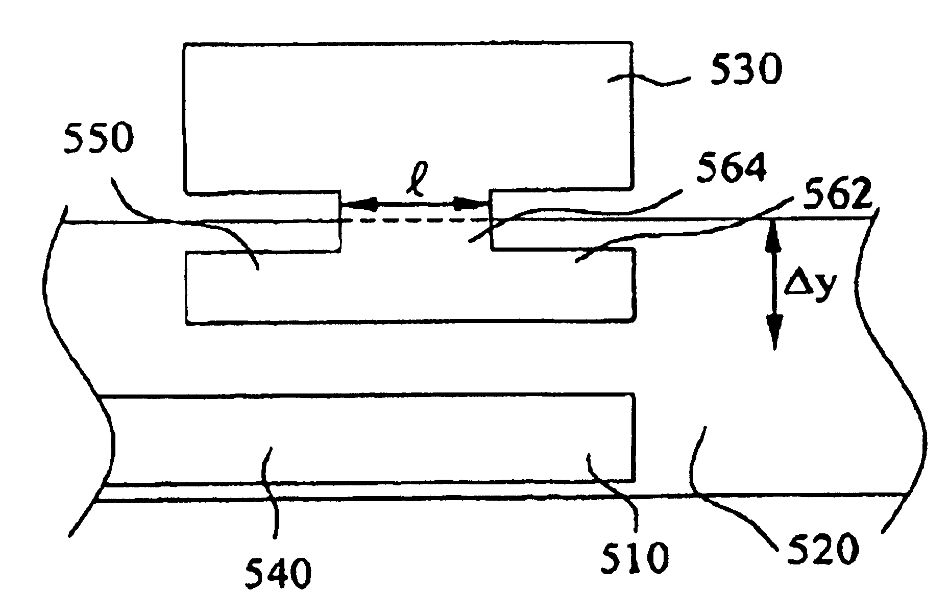
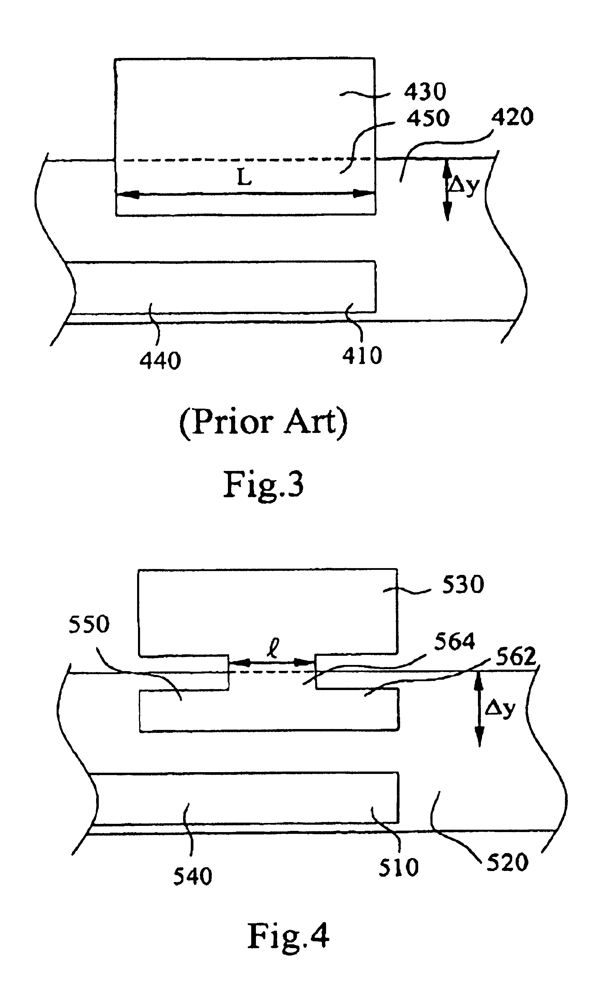
[0017]The functional components on the substrate of the LCD are so arranged that the width of the bridging zone in the direction parallel to the gate electrode peripheral side is smaller than the width of the conducting zone in the same direction parallel to the gate electrode peripheral side. Preferably, the width of the bridging zone in the direction parallel to the gate electrode peripheral side is about within the range between the width of the conducting zone in the same direction parallel to the gate electrode peripheral side and ¼ of the width of the conducting zone in the same direction in parallel to the gate electrode peripheral side. The shape of the projection of the bridging zone and the conducting zone on the gate surface is not limited. Preferably, the bridging zone and the conducting zone are integrated into “T” shape, “L” shape, “Z” shape, or “II” shape. Preferably, the LCD of the present invention comprises an orientation layer coated between the substrate and the ...


PUM


Abstract

A TFT liquid crystal display device is disclosed, which includes two substrates and a liquid crystal layer provided in between the substrates, one substrate having a surface providing with a plurality of data signal lines, a plurality of scan lines, a plurality of pixel electrodes, and a plurality of functional components having source electrode, gate electrodes and drain electrodes. Moreover, the projection of one of the signal electrode and the drain electrode on the gate electrode having at least one bridging zone and one conducting zone. The width of the bridging zone in the direction in parallel to one side of the gate electrode is smaller than the width of the conducting zone in the direction in parallel to the side of the gate electrode.

Description

CROSS-REFERENCE TO RELATED APPLICATION [0001]This application is a reissue of application Ser. No. 10 / 262,899 filed Oct. 3, 2002, U.S. Pat. No. 6,777,750.<?insert-end id="INS-S-00001" ?>BACKGROUND OF THE INVENTION[0002]1. Field of the Invention[0003]The present invention relates to a TFT (thin-film transistor) flat panel display device and its manufacturing method and, more particularly, to a TFT LCD (liquid crystal display) that greatly improves the brilliance.[0004]2. Description of Related Art[0005]In recent years, TFT liquid crystal display devices greatly attract consumer's attention because their advantages such as lighter weight and thinner size. Liquid crystal display devices (LCDs) have been accepted by consumers more and more since the improvement in manufacturing process and prices. However, conventional LCDs still have drawbacks, for example, poor brilliance. The brilliance of a conventional LCD results from many factors. It is well known that the phenomenon of sho...

Claims


Application Information

Patent Timeline
IPC IPC(8): H01L29/04H01L31/036H01L31/20H01L31/0376G02F1/1368
CPCG02F1/1368H01L27/1214
Inventor CHU, HUNG-JENCHANG, MING-HSUANHO, CHIEN-KUOHSIAO, NAI-JEN
Owner CHUNGHWA PICTURE TUBES LTD
Why Eureka
Try Eureka