Circuit board for mounting electronic parts

a technology for electronic components and circuit boards, applied in the field of circuit boards, can solve the problems of difficult to increase the speed of signal transmission between electronic circuit parts to be mounted and the mother board, and dead space where wiring is not possible, so as to avoid the enlargement of the entire board, improve the wiring efficiency, and improve the effect of efficiency

Inactive Publication Date: 2013-06-04
IBIDEN CO LTD
View PDF51 Cites 6 Cited by
  • Summary
  • Abstract
  • Description
  • Claims
  • Application Information

AI Technical Summary

Benefits of technology

[0011]With a view to solving the above-mentioned problems, the present invention has been accomplished, and it is a primary objective of the present invention to improve the wiring efficiency while avoiding the enlargement of the entire board.

Problems solved by technology

The wires for connecting the pads 23 to the pads 24 therefore are longer than necessary, resulting in a poor wiring efficiency.
The use of this wiring board 21 makes it difficult to increase the speed of signal transmission between electronic circuit parts to be mounted and the mother board.
In this case, however, dead space where wiring is not possible is fo

Method used


Image

  • Circuit board for mounting electronic parts
  • Circuit board for mounting electronic parts
  • Circuit board for mounting electronic parts

Examples


first embodiment

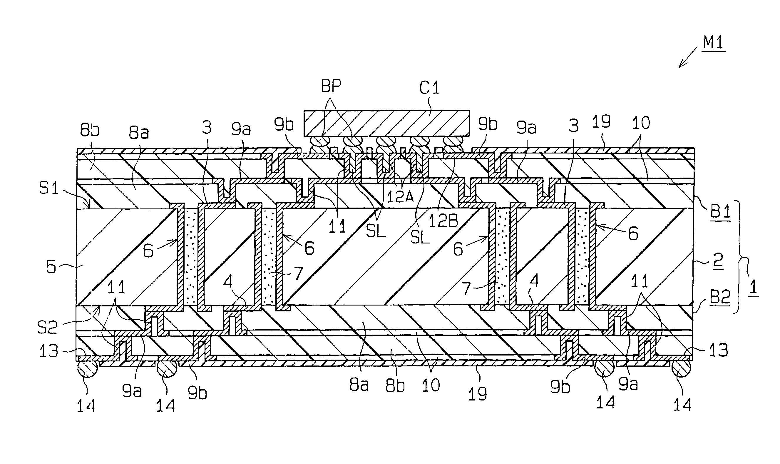
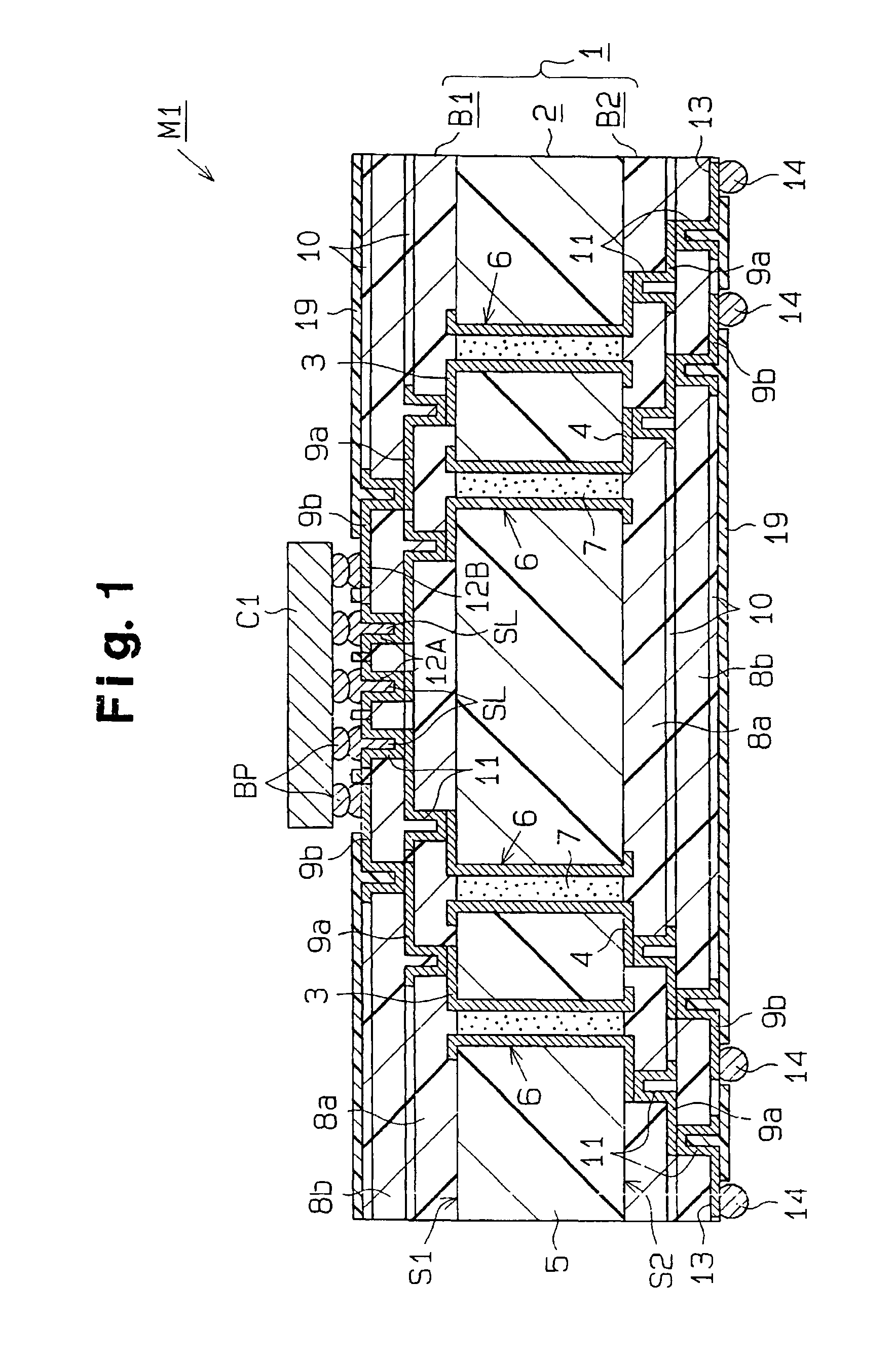
[0033]the present invention will be now described with reference to FIGS. 1 and 2. A wiring board 1 for mounting electronic circuit parts according to this embodiment has a substrate 2 whose top surface S1 and back surface S2 are both usable. The substrate 2 has conductor layers 3 and 4 formed on both the top surface S1 and back surface S2 of a base material 5 of resin by a subtractive method. A plurality of through holes 6 are formed in the substrate 2 to permit the conductor layers 3 and 4 to pass through the substrate 2 and over both the top and back surfaces of the substrate 2. Those through holes 6 are filled with a heat-resistant resin 7.

[0034]Formed on the top surface S1 and the back surface S2 of the substrate 2 are build-up multilayer interconnection layers B1 and B2 each having interlayer dielectric films 8a hand 8b and conductor layers 9a and 9b alternately stacked one on another.

[0035]On the build-up multilayer interconnection layer B1 on the top surface S1, a permanent ...

second embodiment

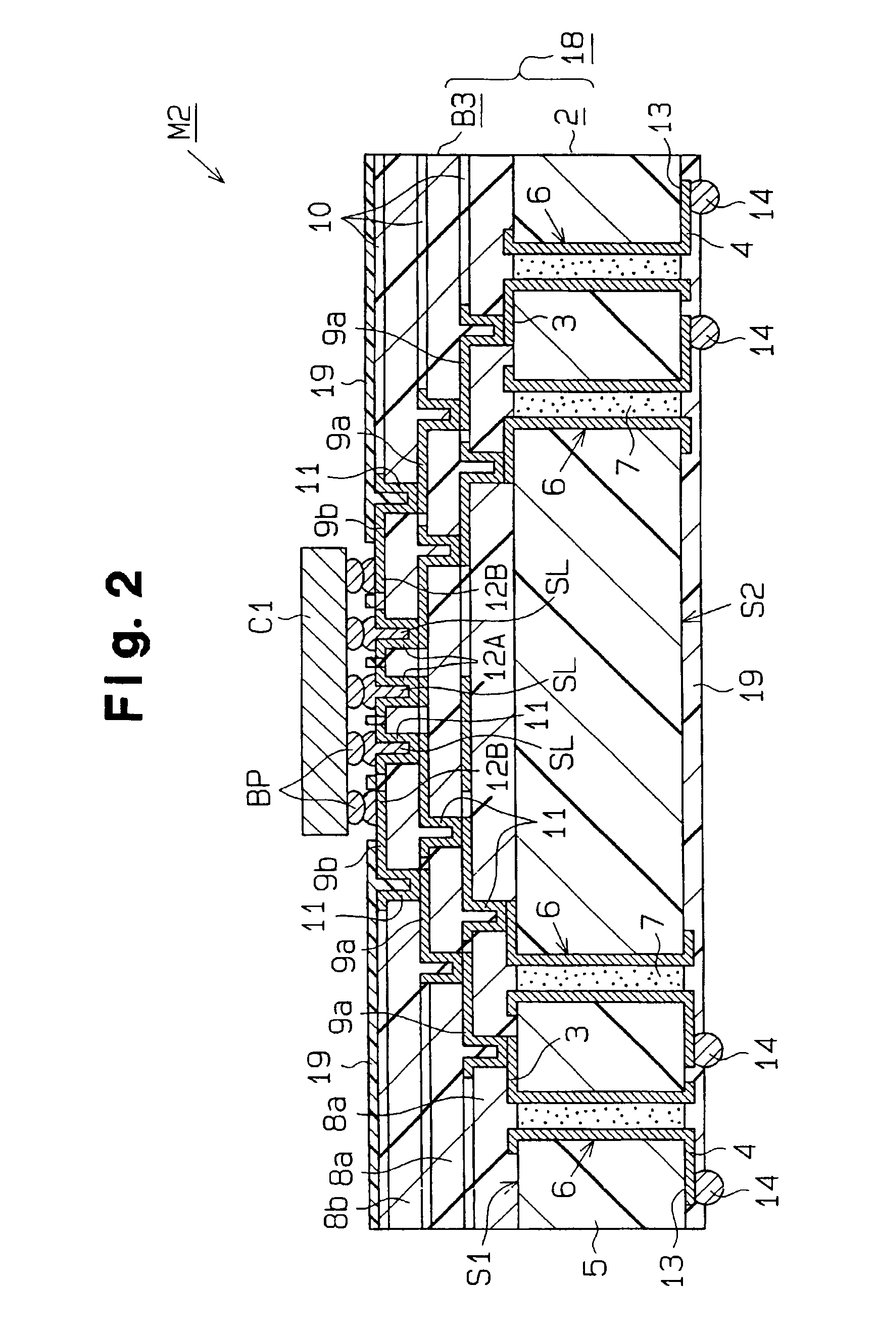
[0118]Next, this invention will be described in detail referring to FIGS. 3 to 7.

[0119]FIG. 3 shows approximately a quarter of a wiring board 51 for mounting electronic circuit parts. The wiring board 51 has a glass epoxy substrate 54 as a core material. It is also possible to employ substrates other than the glass epoxy substrate 54, such as a polyimide substrate and a BT (bismaleimidotriazine) resin substrate. An adhesive layer (dielectric film) 55 is formed on each surface of the substrate 54 using an adhesive specific to the additive method. The surface of each adhesive layer 55 is roughened so as to have a multiplicity of anchoring pits. As the adhesive employable here, a mixture of a photosensitive resin, which can be made hardly soluble in acids or oxidizing agents by a curing treatment, and a cured granular heat-resistant resin soluble in acids or oxidizing agents is employed. The adhesive having such composition is suitable for forming fine images with high accuracy. Detail...


PUM


Abstract

A board for mounting electronic circuit parts includes a first connection terminal group including a plurality of connection terminals densely formed on the top surface of a substrate having through holes formed therein, and a second connection terminal group including a plurality of connection terminals formed at at least the peripheral portion of a back surface of the substrate. The first connection terminal group is connected to the second connection terminal group by way of the through holes. A build-up multilayer interconnection layer having via holes is formed on the top surface of the substrate, so that the first connection terminal group is connected to the second connection terminal group through the build-up multilayer interconnection layer and the through holes. According to another aspect, each signal line on the top surface of the build-up multilayer interconnection layer comprises a plurality of wiring patterns having different widths and a taper-shaped pattern that connects those wiring patterns together and whose width continuously changes. Each signal line has a smaller width at an area having a relatively high wiring density than at an area having a relatively low wiring density.

Description

[0001]This appln is a cont of PCT / JP96 / 02608 filed Sep. 12, 1996 and a cont of Ser. No. 09 / 068,481 filed May 11, 1998 abn.TECHNICAL FIELD[0002]The present invention relates to a board that has connection terminals formed on both the top and back surfaces thereof and on which electronic circuit parts are to be mounted.BACKGROUND ART[0003]A wiring board 21 for mounting electronic circuit parts, as shown in FIG. 8, for example, is known as one conventional printed circuit board for mounting a bare chip like a flip chip or a package like a BGA (Bump Grid Array).[0004]This type of wiring board 21 has a substrate 22 that has conductor layers formed on both the top and back surfaces by mainly a subtractive method. A parts mounting area is provided in the center of the top surface of the substrate 22. Formed densely in this area are multiple pads 23 which constitute a first pad group. The individual pads 23 correspond to bumps BP positioned on the bottom of a bare chip C1.[0005]Multiple pad...

Claims


Application Information

Patent Timeline
IPC IPC(8): H05K1/11H05K3/46H01L23/498H01L23/538H05K1/02H05K3/18
CPCH01L23/49827H01L23/49833H01L23/49838H01L23/49894H01L23/5384H01L2224/16H01L2224/16225H01L2924/01078H01L2924/01079H01L2924/15173H01L2924/15174H01L2924/15311H01R12/523H05K1/0271H05K1/112H05K1/114H05K3/184H05K3/4602H05K3/4661H05K2201/0212H05K2201/09227H05K2201/09472H05K2201/09509H05K2201/09536H05K2201/0959H05K2201/09727H05K2201/10674H05K2201/10734H01L23/12
Inventor ASAI, MOTOOKAWAMURA, YOICHIROMORI, YOJI
Owner IBIDEN CO LTD
Why Eureka
Try Eureka