

Semiconductor light emitting device and manufacturing method for the same
A light-emitting device, semiconductor technology, applied in the direction of semiconductor devices, electrical components, circuits, etc., can solve the problems of current congestion, no contribution to light output, and low luminous efficiency of devices, and achieve the effects of avoiding congestion, improving current expansion, and improving luminous efficiency
- Summary
- Abstract
- Description
- Claims
- Application Information
AI Technical Summary
Problems solved by technology
Method used
Image

Examples
Embodiment 1
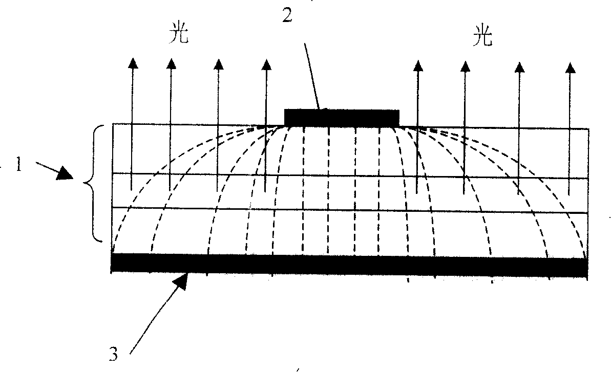
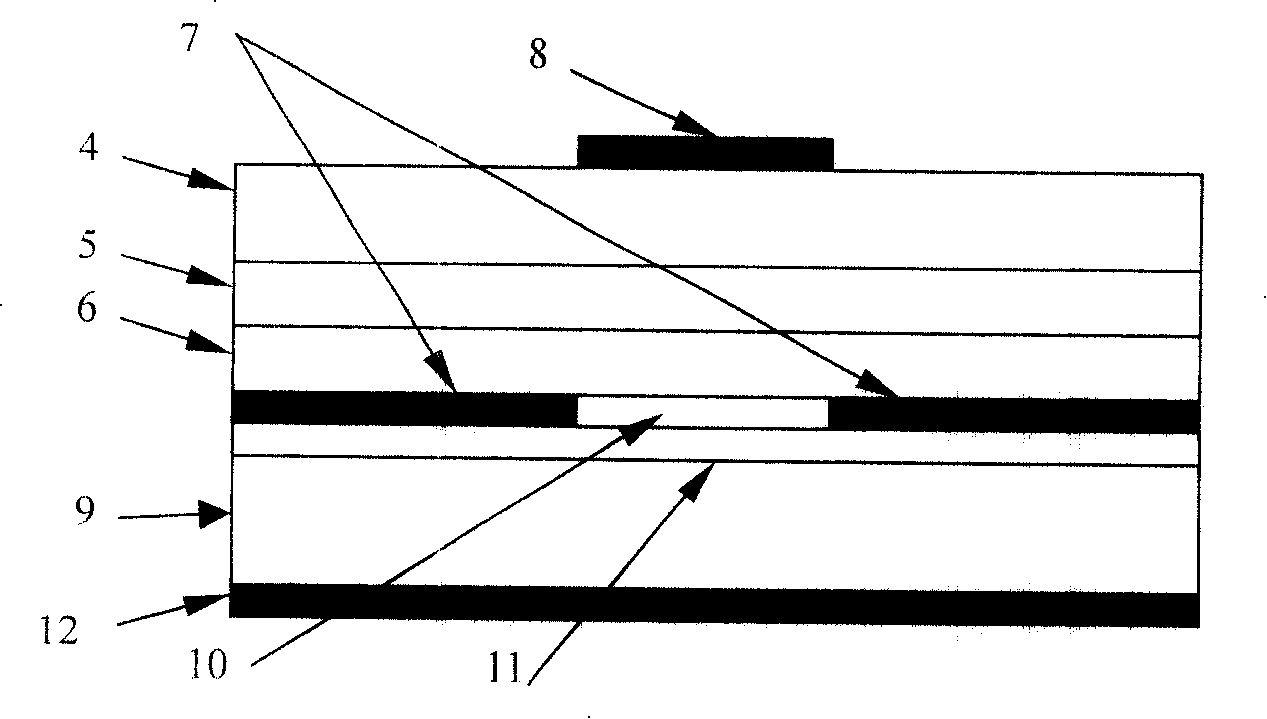
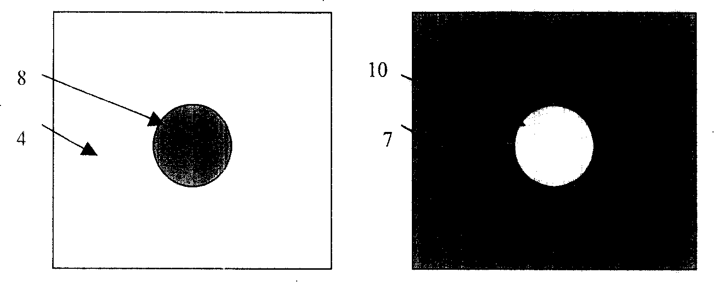
[0052] The semiconductor light emitting device of the present invention, such as figure 2 , image 3 As shown, it includes: a silicon substrate 9 with a main surface and a back surface, an adhesive metal layer 11 stacked on the main surface of the silicon substrate 9, a reflective / The ohmic metal layer 7 is a semiconductor stack stacked on the reflective / ohmic metal layer 7, and the semiconductor stack includes a P-type gallium nitride layer 6, an indium gallium nitride / gallium nitride layer from bottom to top Quantum well light-emitting layer 5 and an N-type gallium nitride layer 4 are stacked on the first ohmic electrode 8 on the N-type gallium nitride layer 4. The ohmic electrode is circular and has a diameter of 100 microns; it is stacked on the silicon The second ohmic electrode 12 on the back of the substrate 9, wherein the reflective / ohmic metal layer 7 has a circular vacancy 10 with a diameter of 100 microns, and the vacancy 10 is filled with a silicon dioxide insul...
Embodiment 2
[0055] The semiconductor light-emitting device of the present invention includes: a silicon substrate 9 having a main surface and a back surface, an adhesive metal layer 11 laminated on the main surface of the silicon substrate 9, and an adhesive metal layer 11 laminated on the adhesive metal layer 11. A reflective / ohmic metal layer 7, a P-type gallium nitride layer 6 stacked on the reflective / ohmic metal layer 7, an indium gallium nitride / gallium nitride multi-quantum layer stacked on the p-type gallium nitride 6 Well light-emitting layer 5, the N-type gallium nitride layer 4 stacked on the InGaN / GaN multi-quantum well light-emitting layer 5, the "meter" layer stacked on the N-type GaN layer 4 The font-shaped first ohmic electrode 8 is stacked on the second ohmic electrode 12 on the back of the conductive substrate 9 , wherein the P-type gallium nitride layer 6 has a "m"-shaped vacancy 10 . Wherein the area of the "meter" font vacancy 10 is 1.5 times of the area of the "m...
Embodiment 3
[0059] The semiconductor light emitting device of the present invention comprises: a silicon substrate 9 having a main surface and a back surface; an adhesive metal layer 11 laminated on the main surface of the silicon substrate 9; an adhesive metal layer 11 laminated on the adhesive metal layer 11 Reflective / ohmic metal layer 7 on top; P-type gallium nitride layer 6 stacked on said reflective / ohmic metal layer 7; Indium gallium nitride / nitride stacked on said P-type gallium nitride layer 6 Gallium light-emitting layer 5; the N-type gallium nitride layer 4 stacked on the light-emitting layer 5; the first ohmic electrode 8 stacked on the N-type gallium nitride layer 4, the shape of the electrode is as follows Image 6 As shown in middle 8; the second ohmic electrode 12 stacked on the back side of the silicon substrate 9, wherein the P-type gallium nitride layer 4 and the light emitting layer 5 all have a vacancy 10, the shape of the vacancy is as follows Image 6 Shown in 10. ...
PUM
 Abstract
Description
Claims
Application Information