
Heat sink for ball single array packaged chip and its application
An array packaging and heat dissipation device technology, which is applied to the combination of ball single array package chips and printed circuit boards, and the field of heat dissipation devices, can solve the problems of increased PCB board cost, increased number of via holes, increased chip manufacturing costs, etc., to achieve excellent heat dissipation High performance, good cooling effect, low cost effect
- Summary
- Abstract
- Description
- Claims
- Application Information
AI Technical Summary
Problems solved by technology
Method used
Image

Examples
no. 1 example
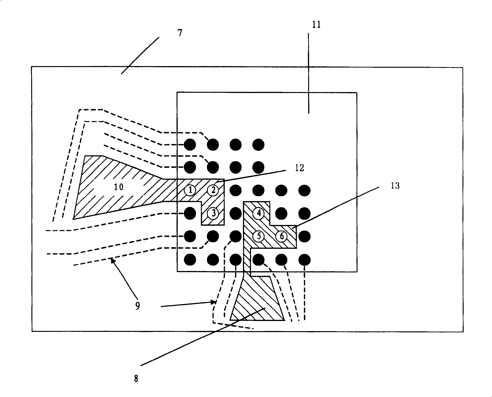
[0041] First embodiment: figure 1 A part of the chip pin arrangement diagram of a BGA chip is given in . This BGA chip 11 has four rows of pins. Among them, pins 1, 2, and 3 are power supply pins whose attribute is power; pins 4, 5, and 6 are ground pins whose attribute is ground; other black pins are signal pins of the BGA chip. Because the copper wires connecting the signal pins are too much and other processing will generate noise and affect the signal transmission quality, so the signal pins for transmitting signals cannot be used for heat dissipation, and the power pins and ground pins only have specific electrical properties, so A heat sink can be added around it to dissipate the heat inside the chip. On the PCB 7 , the signal pins provide electrical signals to the outside through dotted lines. The BGA chip 11 has a definite package size on the PCB 7, and all pins are within the package size.
[0042] figure 1 Among them, the pins 1, 2, and 3 whose attribute is powe...
no. 2 example
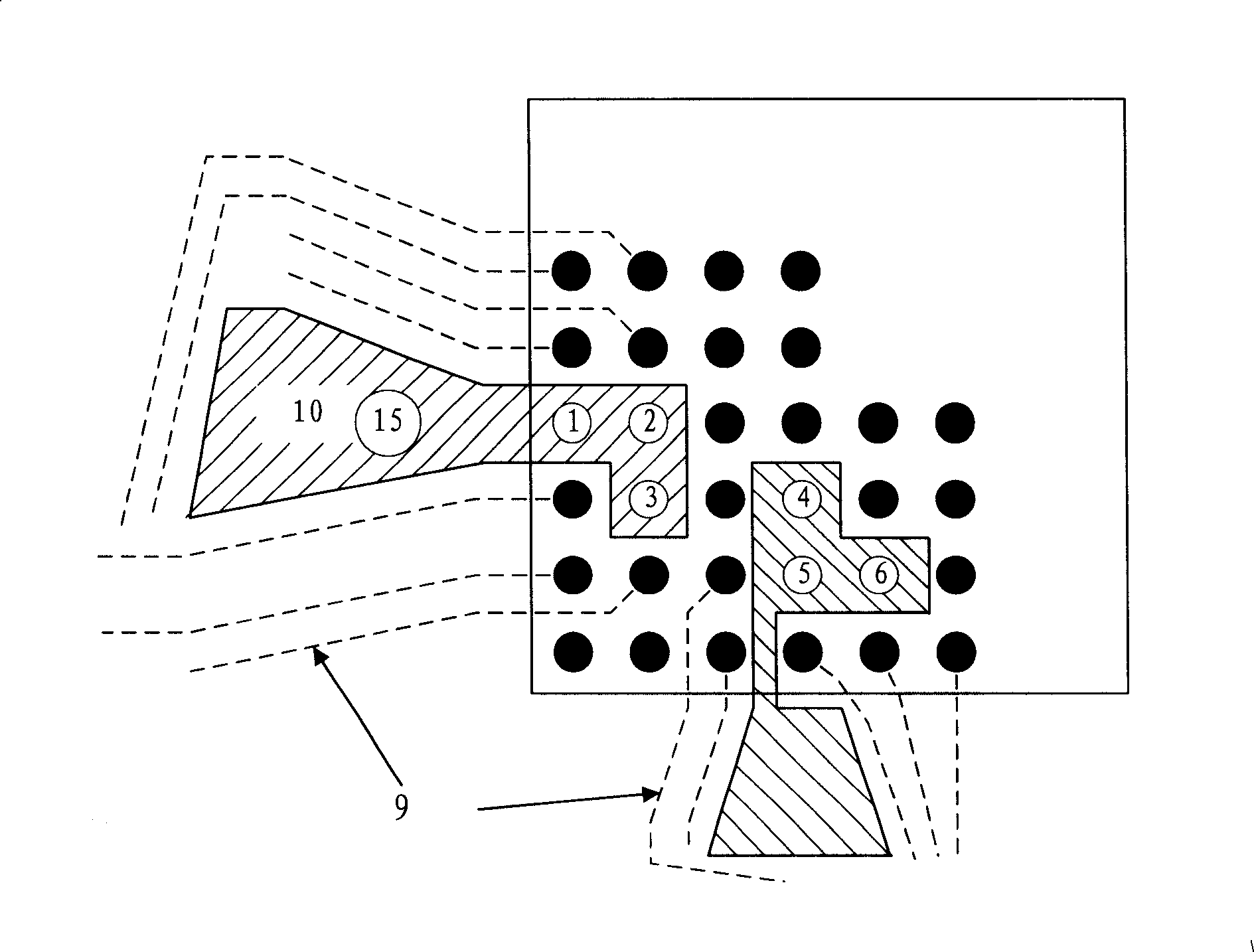
[0045] The second embodiment: with figure 2 shown as an example. The BGA chip 11 has four rows of pins. Among them, pins 1, 2, and 3 are power supply pins whose attribute is power supply; pins 4, 5, and 6 are ground pins whose attribute is ground; other black pins are signal pins of BGA chip; marked in the figure 15 is a via. On the PCB 7 , the signal pins provide electrical signals to the outside through dotted lines. The BGA chip 11 has a definite package size on the PCB 7, and all pins are within the package size. This embodiment describes the process of connecting the large-area copper sheet on the surface layer of the PCB to the power layer of the PCB through via holes to dissipate heat. Since the process of connecting the large-area copper sheet whose electrical property is the ground on the surface layer of the PCB to the ground layer through the via hole can be derived accordingly, it will not be repeated here.
[0046] figure 1 Among them, the pins 1, 2, and 3 ...
PUM
 Abstract
Description
Claims
Application Information