Semiconductor device and open structure of semiconductor device

An opening structure, semiconductor technology, applied in the direction of semiconductor devices, semiconductor/solid-state device manufacturing, semiconductor/solid-state device components, etc., can solve the problems of manufacturing yield impact, increasing process complexity, and inability to provide better step coverage, etc. , to achieve the effect of improving reliability and coverage

Active Publication Date: 2008-09-17
TAIWAN SEMICON MFG CO LTD
View PDF7 Cites 0 Cited by
  • Summary
  • Abstract
  • Description
  • Claims
  • Application Information

AI Technical Summary

Problems solved by technology

[0003] With the development of high-density integrated circuit technology, more components need to be placed on a chip to increase the complexity of the process, while increasing the density and aspect ratio of contact windows
The increase in circuit density also results in an increase in the aspect ratio of contact openings or via openings
However, higher aspect ratios have a negative impact on manufacturing yield because contact openings or via openings need to have better metal step coverage to provide reliable electrical contact
That is, as the aspect ratio increases, the deposition of the barrier layer cannot provide better step coverage due to necking at the top of the contact opening or via opening.

Method used


Image

  • Semiconductor device and open structure of semiconductor device
  • Semiconductor device and open structure of semiconductor device
  • Semiconductor device and open structure of semiconductor device

Examples


Embodiment Construction

[0021] In order to make the above-mentioned purposes, features and advantages of the present invention more obvious and easy to understand, the preferred embodiments are specifically cited below, together with the accompanying drawings, and are described in detail as follows:

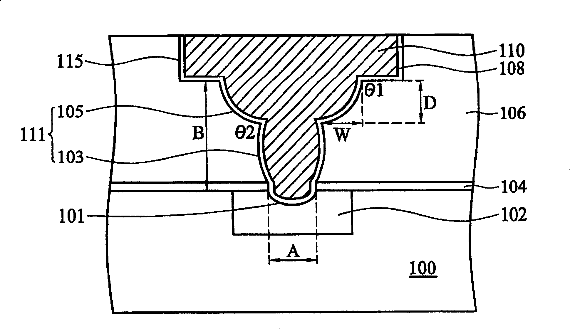
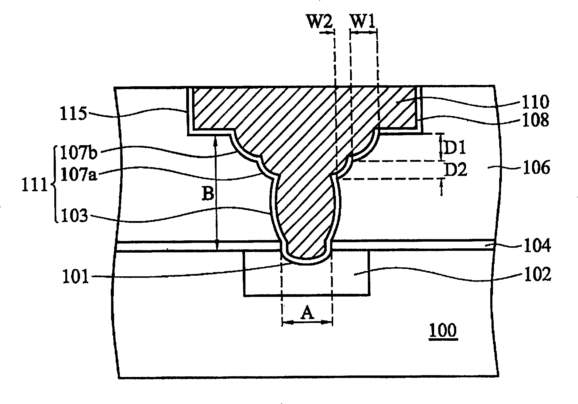
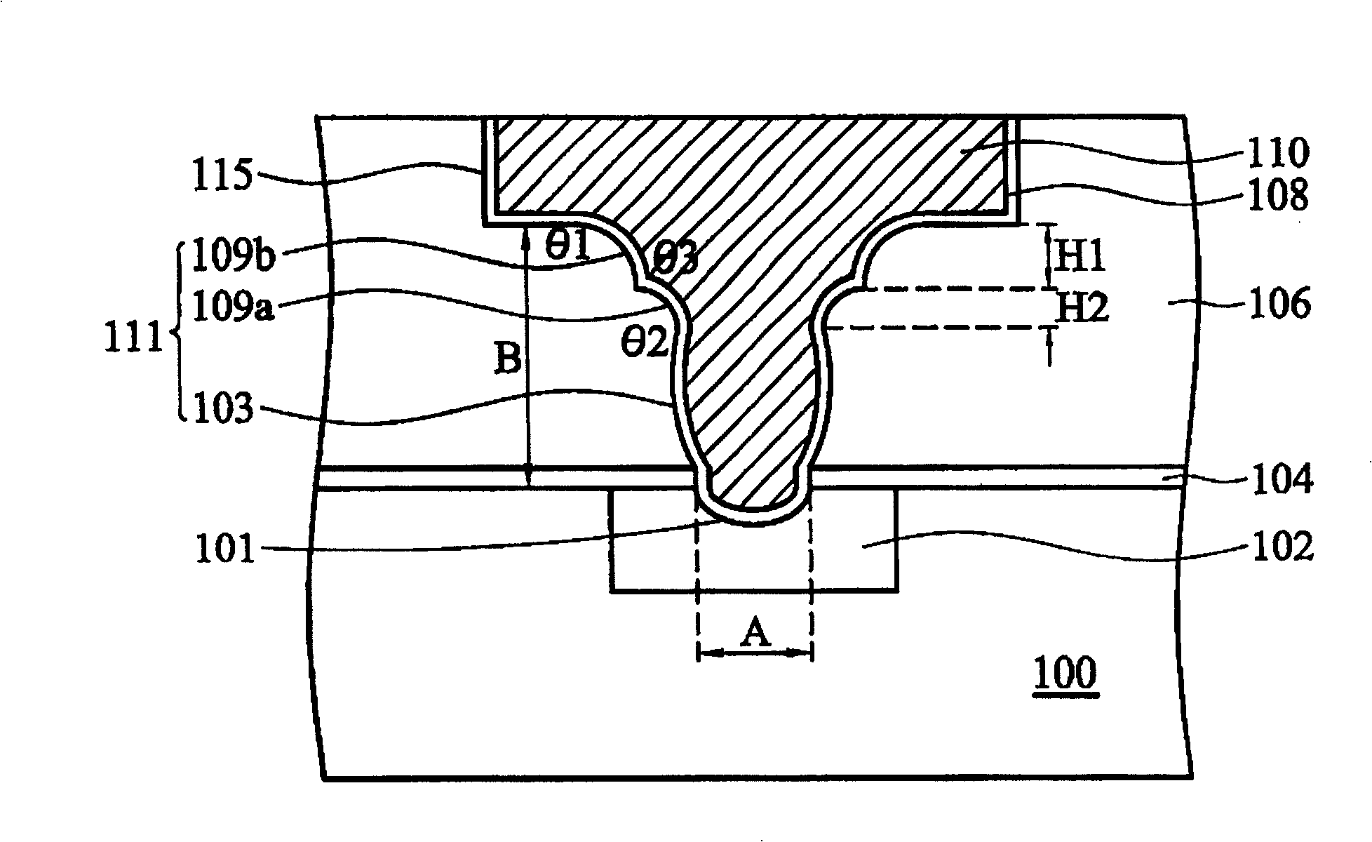
[0022] The present invention relates to an improved via opening suitable for semiconductor devices. The following fit figure 1 A schematic cross-sectional view of a semiconductor device with an opening structure according to an embodiment is shown. The opening structure can be a contact opening structure or a via layer opening structure. The semiconductor device includes a substrate 100 , a dielectric layer 106 and a metal layer 110 . The substrate 100 can be a silicon substrate or other semiconductor substrates, and can include various components therein, such as transistors, resistors, capacitors and other commonly used semiconductor components. Furthermore, the substrate 100 may also include a con...


PUM


Abstract

The present invention provides a semiconductor device and an open structure of the semiconductor device, in particular to an opening structure in a semiconductor device with improved step coverage. The opening structure comprises a dielectric layer overlying a substrate and having at least one via opening to expose the substrate. Wherein the via opening comprises a step region in the upper portion of the via opening and a concave profile region with respect to the dielectric layer in the lower portion of the via opening. The semiconductor device and the open structure of the semiconductor device of the present invention is capable of improving the percentage of coverage of the metal step and further improving the reliability of the device.

Description

technical field [0001] The present invention relates to a semiconductor device, and more particularly to a via opening structure of a semiconductor device, which has a low aspect ratio (aspectratio) and is better for barrier layer deposition. The step coverage (stepcoverage). Background technique [0002] In the manufacture of semiconductor integrated circuits, the fabrication of contact windows is used to electrically connect active regions or conductive layers in the semiconductor substrate. The semiconductor substrate has a metal interconnection layer formed on a dielectric layer, and the dielectric layer is interposed between the substrate and the interconnection layer. In the manufacture of contact windows, contact openings or via openings are usually formed in the dielectric layer to expose the active area or conductive layer, and a conductive plug is filled in it as a layer from the active area or conductive layer to the interconnection layer conduction path between...

Claims


Application Information

Patent Timeline
Patent Type & Authority Patents(China)
IPC IPC(8): H01L23/52H01L21/768
CPCH01L21/76805H01L21/76804H01L21/76816H01L23/485H01L21/76847H01L2924/0002H01L23/5226H01L23/5283H01L2924/00
Inventor 苏怡年谢志宏黄震麟林俊成谢静华眭晓林
Owner TAIWAN SEMICON MFG CO LTD
Why Eureka
Try Eureka