Method for producing MOS transistor with shallow-source electrode/drain electrode junction region

A technology of MOS transistors and junction regions, which is applied in the direction of transistors, semiconductor/solid-state device manufacturing, semiconductor devices, etc., and can solve problems such as difficulty in increasing dopant doping concentration and low resistance in solid-phase diffusion sources

Inactive Publication Date: 2008-10-01
ELECTRONICS & TELECOMM RES INST
View PDF3 Cites 0 Cited by
  • Summary
  • Abstract
  • Description
  • Claims
  • Application Information

AI Technical Summary

Problems solved by technology

The solid phase diffusion method is difficult to increase the doping concentration of the dopant in the solid phase diffusion source enough to make the shallow source / drain junction region have low resistance
In addition, there is the problem of precisely controlling the doping concentration of the dopant in the solid-phase diffusion source

Method used


Image

  • Method for producing MOS transistor with shallow-source electrode/drain electrode junction region
  • Method for producing MOS transistor with shallow-source electrode/drain electrode junction region
  • Method for producing MOS transistor with shallow-source electrode/drain electrode junction region

Examples


Embodiment Construction

[0016] Hereinafter, embodiments of the present invention will be described in detail with reference to the accompanying drawings. However, the embodiments of the present invention can be changed into other forms, and the scope of the present invention is not limited by the embodiments. Rather, the examples are provided in order to more fully explain the present invention to those skilled in the art. In the drawings, the thickness of layers or regions are exaggerated for clarity. Like reference numerals in the figures denote like components. Also, when it is written that a layer is formed "on" another layer or substrate, the layer may be formed directly on the other layer or the substrate, or other layers may be interposed therebetween.

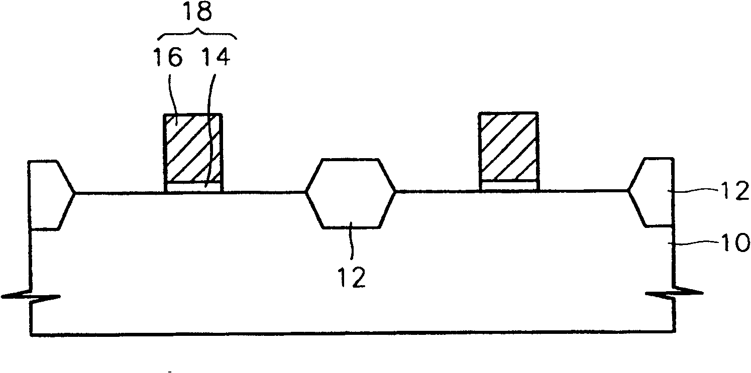
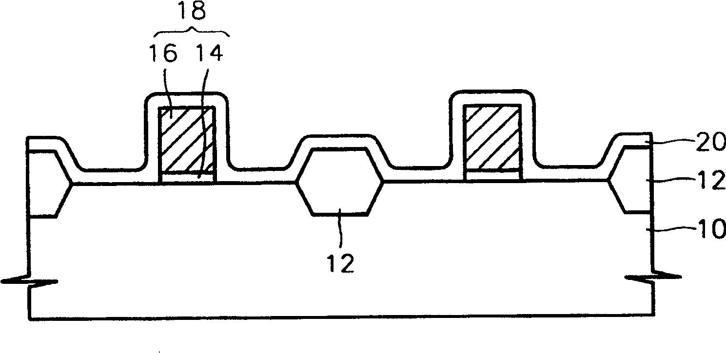
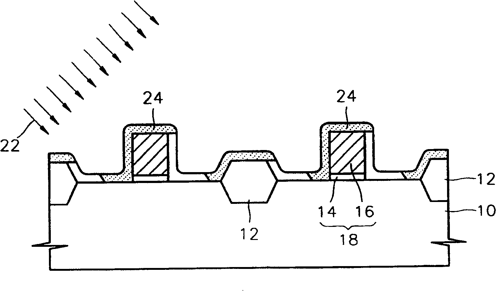
[0017] Figures 1 to 6 is a cross-sectional view illustrating a method of manufacturing a MOS transistor having a shallow source / drain junction region according to a first embodiment of the present invention. refer to figure 1 A field oxi...


PUM


Abstract

A method of fabricating a MOS transistor having shallow source / drain junction regions is provided. A diffusion source layer is formed on a semiconductor substrate on which gate patterns are formed. Same type or different type of impurities are implanted into the diffusion source layer several times in different directions. As a result, dislocation does not occur and the impurity concentration of the diffusion source layer can be nonuniformly controlled so that damage to the crystal structure of the semiconductor substrate does not occur. Also, the impurities nonuniformly contained in the diffusion source layer are diffused into the semiconductor substrate by a solid phase diffusion method to form shallow source / drain junction regions having LDD regions and highly doped source / drain regions by a self-alignment method.

Description

technical field [0001] The present invention relates to a method of manufacturing a MOS transistor, and more particularly, to a method of manufacturing a MOS transistor with a shallow source / drain junction region. Background technique [0002] Generally, a gate pattern including a gate oxide layer and a gate electrode is formed on a semiconductor substrate. A source / drain junction region is formed in the semiconductor substrate under two sidewalls of the gate pattern. As a result, a MOS transistor is formed. [0003] Because MOS transistors are highly integrated, the source / drain junction must be shallow. The shallow junction region must be a junction region which is formed to a shallow depth within the substrate, has impurities of high concentration and high activation rate to reduce resistance, and has a sharp junction shape in the horizontal and vertical directions. [0004] Conventional source / drain junctions are formed by ion implantation or solid phase diffusion. I...

Claims


Application Information

Patent Timeline
Patent Type & Authority Patents(China)
IPC IPC(8): H01L21/22H01L21/265H01L21/336H01L21/8238H01L21/8234H01L21/225H01L21/334H01L27/088H01L27/092H01L29/78
CPCH01L29/7833H01L21/26586H01L29/6659H01L21/823814H01L21/2255H01L21/18
Inventor 李诚宰赵元珠朴京完
Owner ELECTRONICS & TELECOMM RES INST
Why Eureka
Try Eureka