Memory device and method for fabricating the same

A technology for storage devices and storage nodes, which is applied in semiconductor/solid-state device manufacturing, electric solid-state devices, semiconductor devices, etc., and can solve problems such as increased junction leakage current, reduced data retention time, and degradation of recovery characteristics of storage devices

Inactive Publication Date: 2008-11-26
SK HYNIX INC
View PDF3 Cites 0 Cited by
  • Summary
  • Abstract
  • Description
  • Claims
  • Application Information

AI Technical Summary

Problems solved by technology

However, due to excessive ion implantation for obtaining a high doping concentration, the edge region A of the storage node contact junction 170B in the cell region will have a high level of electric field, and thus, the junction leakage current at the junction portion of the storage node contact junction 170B increases.
Such an increase in junction leakage current causes a decrease in data retention time, that is, degradation of the recovery characteristics of the memory device

Method used


Image

  • Memory device and method for fabricating the same
  • Memory device and method for fabricating the same
  • Memory device and method for fabricating the same

Examples


no. 1 example

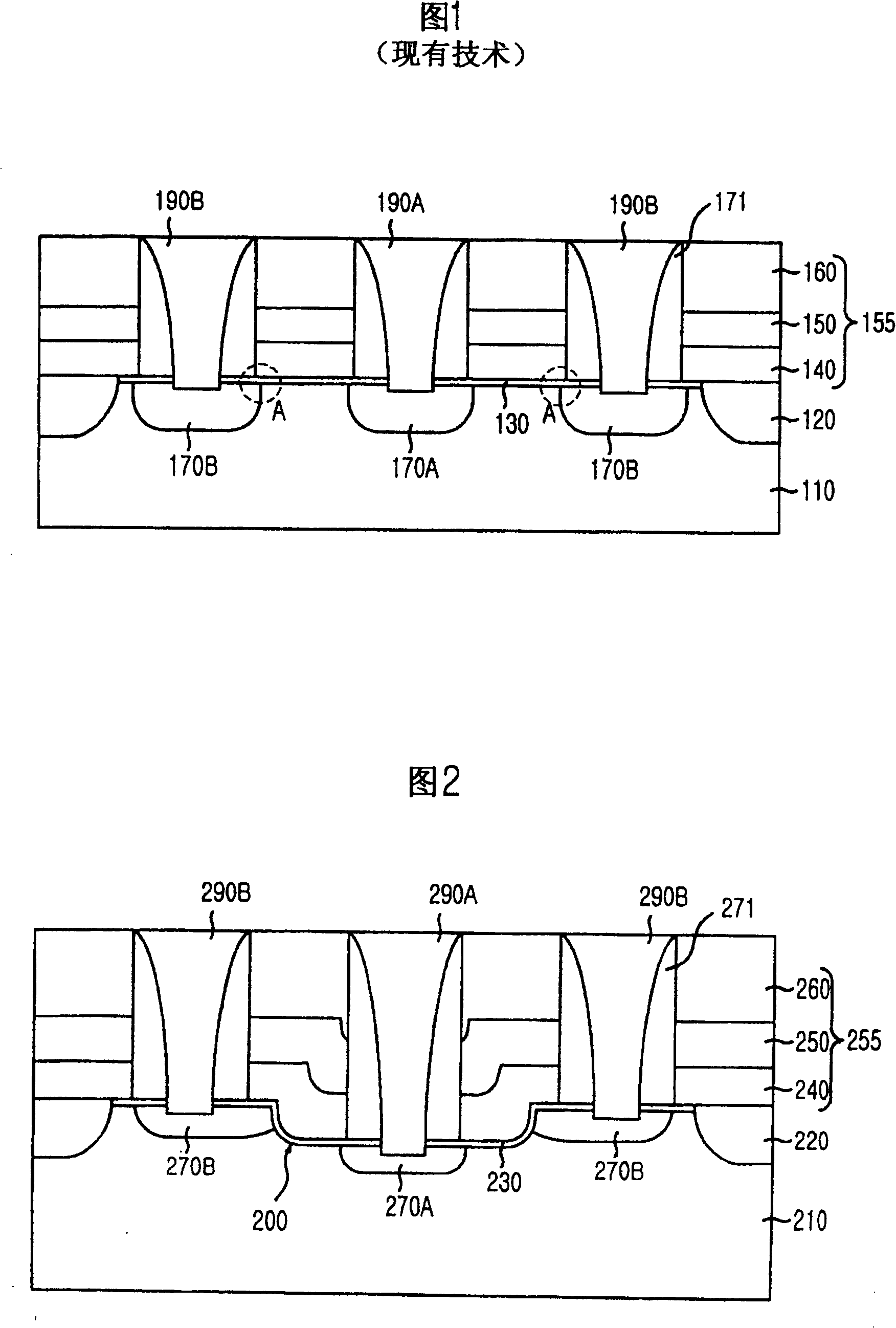
[0037] According to the first embodiment of the present invention, the first contact junction 270A connected to the bit line is formed in the substrate in the trench 200, so the sidewall of the trench 200 constitutes the channel region of the transistor in the cell region.

[0038] Figure 4 A cross-sectional view illustrating a structure of a memory device according to a second embodiment of the present invention.

[0039] Here, the memory device according to the second embodiment includes the same configuration elements described in FIG. 2, and therefore, detailed descriptions about such configuration elements will be omitted. The memory device manufactured according to the second embodiment differs from the memory device manufactured according to the first embodiment in that the side wall B of the trench 300 is formed perpendicular to the surface of the recessed portion of the substrate 310 , and the plurality of gate structures 355, the first contact junction 370A and the s...


PUM


Abstract

Disclosed are a memory device and a method for fabricating the same. The memory device includes: a substrate provided with a trench; a bit line contact junction formed beneath the trench; a plurality of storage node contact junctions formed outside the trench; and a plurality of gate structures each being formed on the substrate disposed between the bit line contact junction and one of the storage node contact junctions. Each sidewall of the trench becomes a part of the individual channels and thus, channel lengths of the transistors in the cell region become elongated. Accordingly, the storage node contact junctions have a decreased level of leakage currents, thereby increasing data retention time.

Description

technical field [0001] The present invention relates to a memory device and a manufacturing method thereof, and more particularly, to a memory device capable of improving data retention time and a manufacturing method thereof. Background technique [0002] As semiconductor devices have been increasingly miniaturized, the size of each pattern has been gradually reduced. Especially in memory devices such as dynamic random access memory (DRAM) devices, due to large-scale integration, the length of the gate electrode is drastically reduced in proportion to the reduction in transistor size in the cell region, and as a gate As a result of the reduction in electrode size, the junction of the source and drain has played an important role in the electric field and potential applied to the body of the transistor in the cell. [0003] FIG. 1 is a cross-sectional view illustrating the structure of a conventional memory device. [0004] As shown, a field oxide layer 120 for isolating d...

Claims


Application Information

Patent Timeline
Patent Type & Authority Patents(China)
IPC IPC(8): H01L27/10H01L27/108H01L21/8239H01L21/8242
CPCH01L29/4933
Inventor 张世亿郑台愚金瑞玟金愚镇朴滢淳金荣福梁洪善孙贤哲黄应林
Owner SK HYNIX INC
Why Eureka
Try Eureka