Method of manufacturing semiconductor device

a manufacturing method and semiconductor technology, applied in the direction of semiconductor devices, basic electric elements, electrical appliances, etc., can solve the problems of deterioration of the uniformity of the sheet resistance, increase in and local formation of the silicide film on the surface, so as to prevent the variation of the sheet resistance of the silicide film and reduce the junction leakage current

Inactive Publication Date: 2013-05-07
RENESAS ELECTRONICS CORP
View PDF7 Cites 0 Cited by
  • Summary
  • Abstract
  • Description
  • Claims
  • Application Information

AI Technical Summary

Benefits of technology

[0023]According to this configuration, since the formation of the silicide film and the formation of the metal oxide film are simultaneously performed, and in the thermal oxidation treatment step, since the surface of the metal film is oxidized while performing the silicide reaction, reaction causing the generation of the oxide at the time of selectively removing the unreacted metal film later using a sulfuric hydrogen peroxide mixture can prevent the insufficient silicide film from being formed. In addition, since the metal oxide is formed by oxidizing even the surface side of the metal film located on the insulating film, it is possible to prevent an extra metal material from flowing into the silicon region, and to prevent the abnormal growth from being generated.
[0025]According to the invention, it is possible to prevent variation of the sheet resistance of the silicide film and to reduce the junction leakage current of the semiconductor device including the silicide film.

Problems solved by technology

However, in the past, for example, in the method disclosed in Japanese Unexamined Patent Publication No. 2009-111214, there has been a problem that a Si oxide 12 (see FIGS. 9A and 9B) is locally formed on the surface of the silicide film.
First, since silicide reaction by initial annealing is insufficient, the silicide film richer in Ni (richer in metal) than Ni2Si is locally formed at the surface side of the silicide film.
In addition, especially, when thinning of the silicide film proceeds, there also occurs a problem that abnormal growths 13 (see FIG. 9B) is easily generated in the direction of the interface of the silicide film 9 with an STI 2 or the direction of the interface thereof with the sidewall 4, and an increase in a junction leakage current or uniformity of the sheet resistance is deteriorated.
However, in this method, the formation of the oxide 12 or the generation of the abnormal growth 13, as mentioned above, cannot be prevented.

Method used


Image

  • Method of manufacturing semiconductor device
  • Method of manufacturing semiconductor device
  • Method of manufacturing semiconductor device

Examples


example)

(Example)

[0061]The second silicide film 111 was formed on the N-type source / drain region 107 by the same procedure as described in the above-mentioned embodiment, and the sheet resistance and the junction leakage current of the second silicide film 111 were measured.

[0062]Here, the first annealing was performed by the lamp annealing method, under the oxygen atmosphere (concentration of oxygen of 100%), at a temperature of 260° C., for 30 seconds. FIG. 3 shows the measurement result of the sheet resistance in a diffusion layer having a width of 1 μm (shown by (a) in the drawing). The horizontal axis in FIG. 3 denotes sheet resistance ([Ohm / Sq.]), and the vertical axis denotes cumulative probability ([%]). In addition, FIG. 4 shows the measurement result of the junction leakage current in a minute diffusion layer, having a width of equal to or less than 100 nm, which is adjacent to the gate electrode and the STI. The horizontal axis in FIG. 4 denotes the junction leakage current ([A])...

second embodiment

(Second Embodiment)

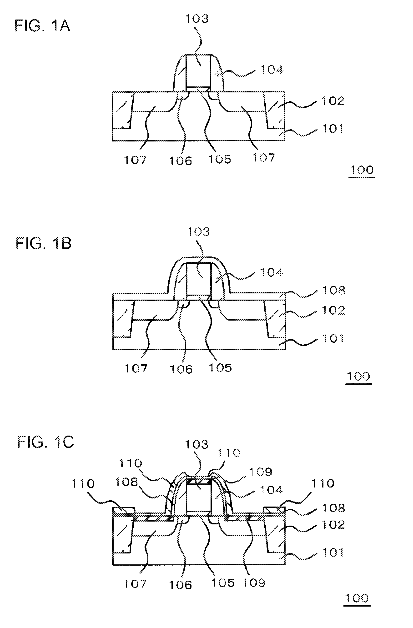
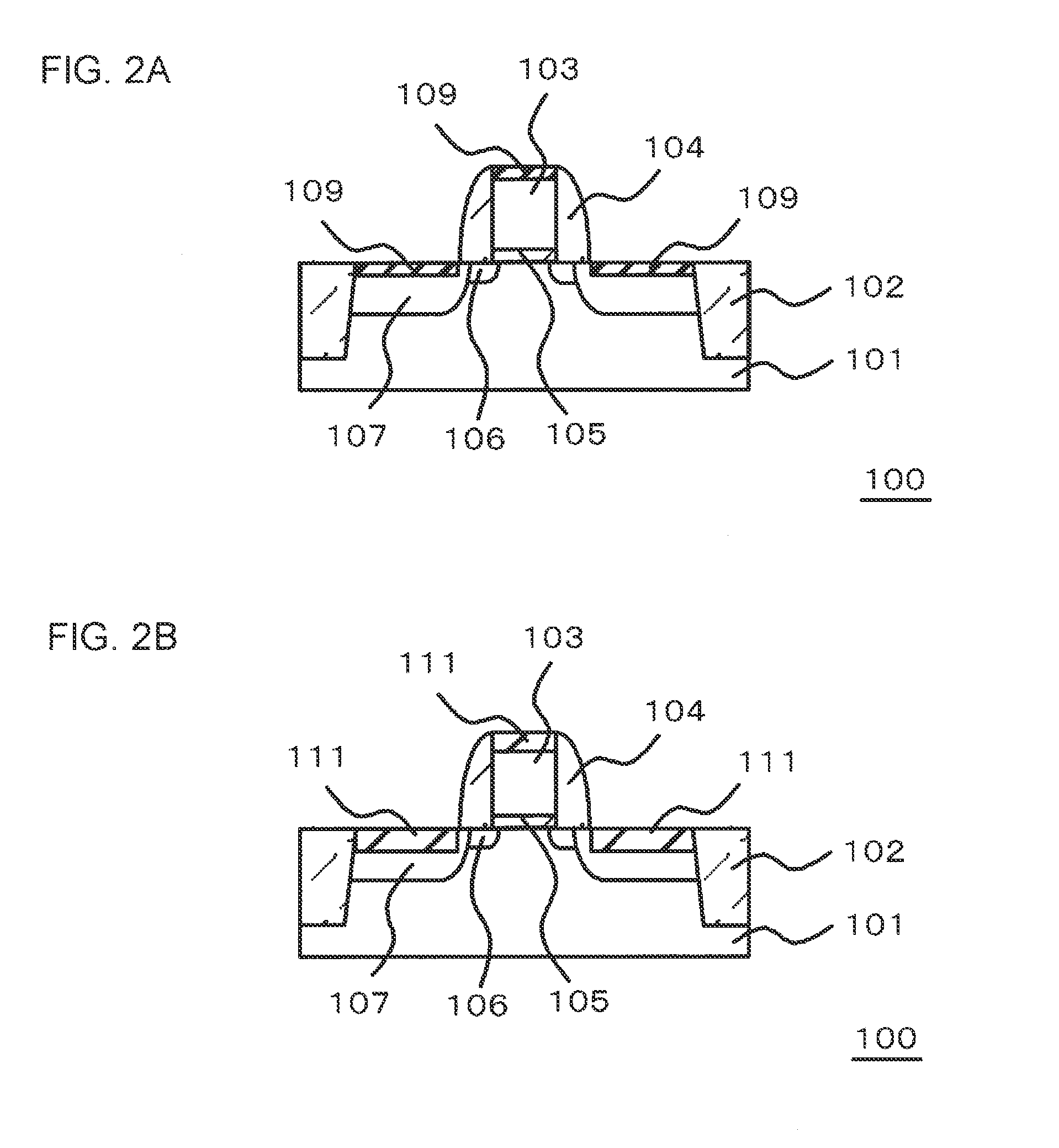
[0075]FIGS. 5A and 5B to FIGS. 7A and 7B are process cross-sectional views illustrating an example of the procedures for manufacturing the semiconductor device 100 according to the embodiment.

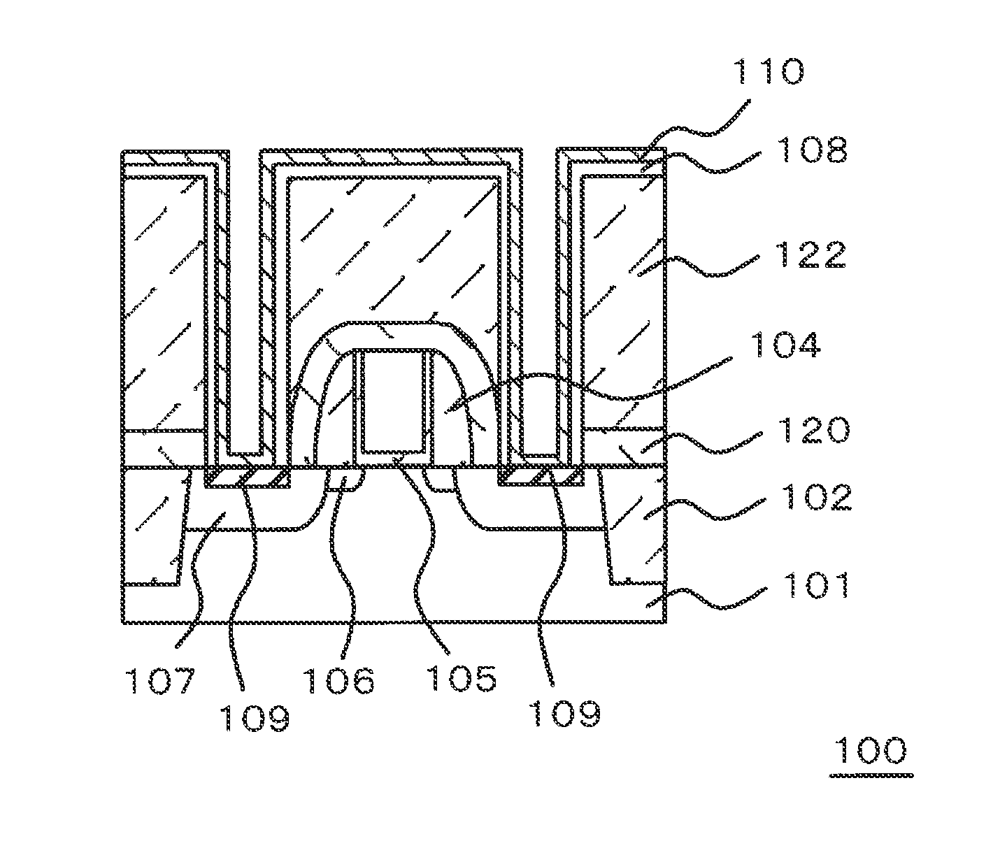
[0076]First, using a well-known method, the semiconductor element is created by forming, on the, silicon substrate 101, the STI 102 used as an element isolation insulating film, a gate electrode 103, the sidewall 104, the gate insulating film 105, the extension region 106, and the source / drain region 107. Meanwhile, the source / drain region 107 can be formed of materials such as SiGe and SiC. Next, a liner insulating film 120 and an insulating interlayer 122 are formed on the entire surface of the silicon substrate 101, and the insulating film is planarized by a chemical mechanical polishing (CMP) method (FIG. 5A). In the embodiment, the gate electrode 103 can be formed of, for example, a metal material.

[0077]Subsequently, using a photolithographic technique and a reactive ion...


PUM

PropertyMeasurementUnit
temperatureaaaaaaaaaa

Abstract

The method of manufacturing a semiconductor device comprises forming a metal film over silicon regions and insulating films; performing a first heat treatment under an oxygen atmosphere containing oxygen as a main ingredient, to form a first silicide film in the silicon region by reacting the metal film and the silicon region, and to simultaneously form a metal oxide by oxidizing the entire surface of the metal film from the surface side thereof; and selectively removing the metal oxide and the unreacted metal film using a chemical.

Description

[0001]This application is based on Japanese patent application No. 2010-074594, the content of which is incorporated herein by reference.BACKGROUND[0002]1. Technical Field[0003]The present invention relates to a method of manufacturing a semiconductor device, and specifically to a method of manufacturing a semiconductor device including a step of forming a silicide film.[0004]2. Related Art[0005]As high integration of semiconductor elements proceeds, it is required that the gate dimensions of a transistor or the interconnect width thereof is miniaturized, and the resistance of gate and source / drain regions decreases for high-speed operation of the transistor. As a technique for solving such a requirement, a salicide process is used in which the resistance of the gate and source / drain regions made of polysilicon is reduced by forming a low-resistance silicide compound of a metal and silicon in a self-aligned manner.[0006]In the salicide process, metals such as Ni, Co, and Ti are form...

Claims


Application Information

Patent Timeline
Patent Type & Authority Patents(United States)
IPC IPC(8): H01L21/336
CPCH01L21/28052H01L21/28518H01L29/41725H01L21/76814H01L2221/1063H01L29/665
Inventor TONEGAWA, TAKASHIMORITA, TOMOTAKEMATSUZAKA, NORIHIKO
Owner RENESAS ELECTRONICS CORP
Why Eureka
Try Eureka