P-type FET and manufacturing method thereof

A manufacturing method, N-type technology, applied in semiconductor/solid-state device manufacturing, electrical components, circuits, etc., can solve the problems of inability to further reduce device leakage and increase junction leakage current, and achieve the goal of eliminating subthreshold leakage current and junction leakage Effect

Active Publication Date: 2020-07-28
SHANGHAI HUALI INTEGRATED CIRCUTE MFG CO LTD
View PDF6 Cites 0 Cited by
  • Summary
  • Abstract
  • Description
  • Claims
  • Application Information

AI Technical Summary

Problems solved by technology

There is a contradiction between reducing the leakage current corresponding to I1 and I2 and the leakage current corresponding to I3 and I4 in existing devices, that is, there is a contradiction in the doping control requirements of the halo implantation region 106: when increasing the doping concentration of the halo implantation region 106 , although the subthreshold leakage current can be reduced, the junction leakage current will increase; and when the doping concentration of the halo implantation region 106 is reduced, the subthreshold leakage current will increase
This leads to the fact that the existing device structure cannot further reduce the leakage of the device

Method used


Image

  • P-type FET and manufacturing method thereof
  • P-type FET and manufacturing method thereof
  • P-type FET and manufacturing method thereof

Examples


Embodiment Construction

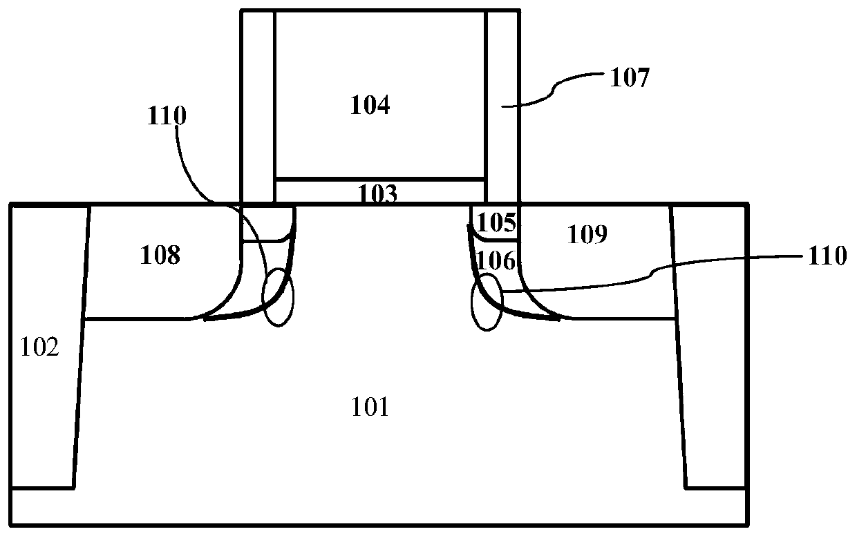
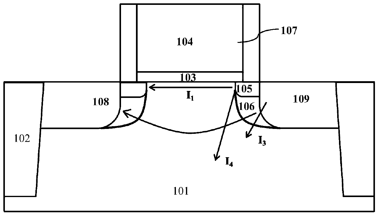
[0070] Such as Figure 4 Shown is a schematic diagram of the structure of the P-type FET of the embodiment of the present invention; the P-type FET of the embodiment of the present invention includes a gate structure, a side wall 7, a channel region, a P-type lightly doped drain region 5, a source region 8, and a drain region. region 9 and halo implant region 6.

[0071] The gate structure is formed on the surface of the semiconductor substrate 1 . Field oxygen 2 is also formed on the semiconductor substrate 1, and the field oxygen 2 isolates an active region.

[0072] An N-type well is formed on the semiconductor substrate 1, the formation region of the P-type FET is located in the formation region of the N-type well, and the gate structure is formed on the surface of the N-type well; N The channel region doped with the N type is composed of the N-type well located between the lightly doped drain regions 5 and between the source region 8 and the drain region 9 and covered b...


PUM


Abstract

The invention discloses a P-type FET. A halo injection region comprises first halo injection sub-regions capable of independently adjusting sub-threshold leakage current and second halo injection sub-regions capable of independently adjusting drain terminal junction leakage current; the junction depth of the first halo injection sub-regions is larger than that of the lightly doped drain regions but smaller than that of the drain regions, the first halo injection sub-regions transversely extend into the channel regions outside the side surfaces of the corresponding lightly doped drain regions,and the first halo injection sub-regions wrap the bottom surfaces and the side surfaces of the lightly doped drain regions; the junction depth of the second halo injection sub-regions is larger than that of the first halo injection regions, the second halo injection sub-regions are located on the inner sides of the side faces of the lightly doped drain regions and located at the bottoms of the lightly doped drain regions, and the second halo injection sub-regions wrap the side faces, located at the bottoms of the lightly doped drain regions, of the corresponding source regions or drain regions. The invention further discloses a manufacturing method of the P-type FET. According to the invention, sub-threshold leakage current and junction leakage current of the device can be reduced at the same time, and extremely low electric leakage is realized.

Description

technical field [0001] The invention relates to the field of semiconductor integrated circuit manufacturing, in particular to a P-type FET. The invention also relates to a method for manufacturing a P-type FET. Background technique [0002] As the size of semiconductor devices continues to shrink, the short-channel effect of devices becomes more and more obvious, making the leakage of devices more and more difficult to control. Especially when the process node enters the nanometer scale, the threshold voltage (Vt) of the device rolls down (roll-off) strongly, making it difficult to control the subthreshold leakage. Although increasing the amount of halo ion implantation can alleviate the problem of subthreshold leakage to a certain extent, a new problem of high leakage at the P-N junction will be introduced when the implant amount is high, resulting in extreme The development of low-leakage components has encountered serious obstacles. [0003] Such as figure 1 As shown,...

Claims


Application Information

Patent Timeline
Patent Type & Authority Applications(China)
IPC IPC(8): H01L29/78H01L29/06H01L29/36H01L21/336
CPCH01L29/7833H01L29/7838H01L29/0607H01L29/0684H01L29/36H01L29/66492H01L29/66575
Inventor 白文琦王世铭黄志森胡展源李昆鸿
Owner SHANGHAI HUALI INTEGRATED CIRCUTE MFG CO LTD
Why Eureka
Try Eureka