
Semiconductor device and method of forming the same

A semiconductor and device technology, applied in the field of semiconductor devices and their formation, can solve problems such as poor electrical performance, achieve the effects of balancing performance, improving carrier mobility, and reducing junction leakage current

Active Publication Date: 2019-07-02
SEMICON MFG INT (SHANGHAI) CORP +1
View PDF3 Cites 0 Cited by
  • Summary
  • Abstract
  • Description
  • Claims
  • Application Information

AI Technical Summary

Problems solved by technology

[0005] However, the semiconductor devices formed by the prior art still have the problem of poor electrical performance

Method used


Image

  • Semiconductor device and method of forming the same
  • Semiconductor device and method of forming the same
  • Semiconductor device and method of forming the same

Examples


Embodiment Construction

[0033] It can be seen from the background art that the electrical performance of semiconductor devices formed in the prior art needs to be improved.

[0034] After research, it is found that the operating voltage (Vdd) of the core device and the input / output device in the semiconductor device is quite different. For example, when the operating voltage of the core device is about 0.8V, the operating voltage of the input / output device is about 1.8V or Around 3.3V. Due to the large difference in operating voltage, the junction leakage current (junction leakage) of the core device and the input / output device is also significantly different. When the operating voltage of the core device is around 0.8V, the junction leakage current of the core device is between 0.1pA / μm and 100pA / μm, and when the operating voltage of the input / output device is around 1.8V, the junction leakage current will be greater than 10000pA / μm.

[0035] Therefore, there is an urgent need to solve the problem ...


PUM


Abstract

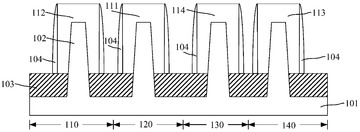
The invention discloses a semiconductor device and a forming method thereof. The forming method of the semiconductor device comprises the steps as follows: a first ion implantation process is carried out on a substrate in a PMOS peripheral region at two sides of a first gate structure and a first graded junction region is formed at the lower part of a first peripheral source-drain region; a second ion implantation process is carried out on the first peripheral source-drain region and a first core drain-source region, and a first contact resistance region is formed on the surface of the first peripheral source-drain region and the surface of the first core drain-source region; a third ion implantation process is carried out on the substrate in an NMOS peripheral region at two sides of a third gate structure and a second graded junction region is formed at the lower part of a second peripheral source-drain region; and a fourth ion implantation process is carried out on a second peripheral source-drain region and a second core drain-source region, and a second contact resistance region is formed on the surface of the second peripheral source-drain region and the second core drain-source region. According to the semiconductor device, the problem of a short channel effect of a core device is solved while junction leakage current of an input / output device is reduced, thereby improving the electric property of the formed semiconductor device.

Description

technical field [0001] The invention relates to the technical field of semiconductor manufacturing, in particular to a semiconductor device and a forming method thereof. Background technique [0002] A Metal-Oxide-Semiconductor (MOS, Metal-Oxide-Semiconductor) device has been known as one of the commonly used semiconductor devices in integrated circuits. The MOS device includes: P-type metal oxide semiconductor (PMOS, P-type MOS) device, N-type metal oxide semiconductor (NMOS, N-type MOS) device and complementary metal oxide semiconductor (CMOS, Complementary MOS) device. [0003] Metal oxide semiconductor devices are mainly divided into core (Core) devices and peripheral (I / O) devices (or called input / output devices) according to functional distinctions. According to the electrical type of metal oxide semiconductor devices, core devices can be divided into core NMOS devices and core PMOS devices, and input / output devices can be divided into input / output NMOS devices and i...

Claims


Application Information

Patent Timeline
Patent Type & Authority Patents(China)
IPC IPC(8): H01L21/8238H01L21/265
CPCH01L21/265H01L21/8238
Inventor 李勇
Owner SEMICON MFG INT (SHANGHAI) CORP
Learn More