Semiconductor structure and manufacturing method thereof

A manufacturing method and semiconductor technology, applied in semiconductor/solid-state device manufacturing, semiconductor devices, transistors, etc., can solve the problems of semiconductor device electrical performance to be improved, achieve the effect of reducing junction leakage current and optimizing electrical performance

Active Publication Date: 2020-08-07
SEMICON MFG INT (SHANGHAI) CORP +1
View PDF4 Cites 0 Cited by
  • Summary
  • Abstract
  • Description
  • Claims
  • Application Information

AI Technical Summary

Problems solved by technology

[0004] However, the electrical properties of semiconductor devices formed by prior art still need to be improved

Method used


Image

  • Semiconductor structure and manufacturing method thereof
  • Semiconductor structure and manufacturing method thereof
  • Semiconductor structure and manufacturing method thereof

Examples


Embodiment Construction

[0014] It can be seen from the background art that in order to improve short-channel effects (SCE: short-channel effects) of devices, the semiconductor process gradually begins to transition from planar MOSFET transistors to three-dimensional transistors (such as FinFETs). However, the electrical performance of the FinFET formed by the prior art still needs to be improved.

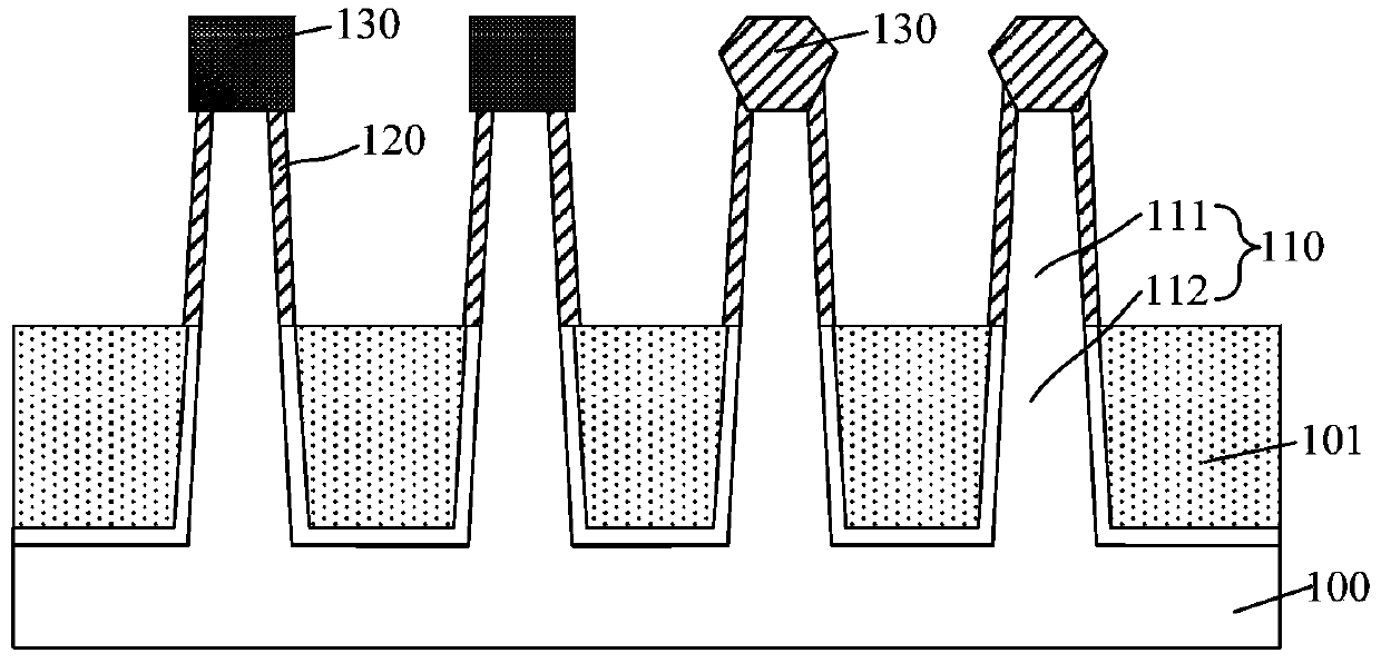
[0015] Combined with the semiconductor structure to analyze the reasons for the above problems in FinFET, refer to figure 1 , shows a schematic structural view of a semiconductor structure.

[0016] The semiconductor structure includes: a substrate 100 and a plurality of discrete fins 110 protruding from the substrate 100; and an isolation structure 101 located on the substrate 100 between the fins 110, wherein, exposed The fin 110 of the isolation structure 101 is used as the first fin region 111, and the unexposed part is used as the second fin region 112; the semiconductor structure further includes a ...


PUM


Abstract

The invention relates to a semiconductor structure and a manufacturing method thereof. The method comprises the steps of providing a base, wherein the base comprises a first depth region, a second depth region and a third depth region; forming a buffer doping ion region in the base of the second depth region; removing a part of the base of the second depth region and the third depth region to form a substrate and fin parts protruding out of the substrate; forming an isolation structures with thickness equal to the depth of the second depth region on the substrate, wherein the fin part exposed out of the isolation structure is a fin part first region, and a part which is not exposed is a fin part second region; forming a punchthrough-prevention doping ion region with an ion type same as that of the buffer doping ion region in the fin part second region, wherein the ion concentration of the punchthrough-prevention doping ion region is larger than that of the buffer doping ion region; forming a grid structure bridging the fin parts; and forming a source-drain doping region in the fin part first region at two sides of the grid structure. The ion concentration of the punchthrough-prevention doping ion region is between that of the source-drain doping region and that of the buffer doping ion region, and thus, the junction leak current between the source-drain doping region and the substrate is reduced.

Description

technical field [0001] The invention relates to the field of semiconductors, in particular to a semiconductor structure and a manufacturing method thereof. Background technique [0002] In semiconductor manufacturing, with the gradual development of ultra-large-scale integrated circuits, the feature size of integrated circuits continues to decrease. In order to adapt to the reduction of feature size, the channel length of MOSFET field effect transistors is also continuously shortened accordingly. However, as the channel length of the device is shortened, the distance between the source and the drain of the device is also shortened, so the control ability of the gate to the channel becomes worse, and the gate voltage pinches off the channel. The difficulty is also increasing, making the phenomenon of subthreshold leakage (subthreshold leakage), the so-called short-channel effect (SCE: short-channel effects) more likely to occur. [0003] Therefore, in order to better adapt ...

Claims


Application Information

Patent Timeline
Patent Type & Authority Patents(China)
IPC IPC(8): H01L21/8234H01L27/088H01L29/10H01L29/78
CPCH01L21/823431H01L27/0886H01L29/1083H01L29/785H01L21/823821H01L29/66803
Inventor 周飞
Owner SEMICON MFG INT (SHANGHAI) CORP
Why Eureka
Try Eureka