MOS transistor and forming method thereof

A MOS transistor and semiconductor technology, applied in the fields of semiconductor devices, semiconductor/solid-state device manufacturing, electrical components, etc., can solve the problems of increasing the thermal budget of semiconductor devices, increasing the process cost, unfavorable ultra-small devices, etc., to reduce junction leakage current, The effect of improving performance and suppressing diffusion effects

Active Publication Date: 2011-03-23
SEMICON MFG INT (SHANGHAI) CORP
View PDF1 Cites 0 Cited by
  • Summary
  • Abstract
  • Description
  • Claims
  • Application Information

AI Technical Summary

Problems solved by technology

[0012] However, in the above process, the transient enhanced diffusion effect is suppressed by adding a thermal annealing process. The annealing temperature is 1000°C and the time is 10 seconds. Annealing at such a high temperature, although the annealing time is short, will also increase the heat of the semiconductor device. budget, greatly increasing the process cost
At the same time, as the device becomes smaller and the ultra-shallow junction is required, thermal annealing is used to suppress the transient enhanced diffusion effect, which itself will cause further diffusion of impurities, and its effect on suppressing the TED effect is also limited, which is not conducive to the development of ultra-small devices. form

Method used


Image

  • MOS transistor and forming method thereof
  • MOS transistor and forming method thereof
  • MOS transistor and forming method thereof

Examples


Embodiment Construction

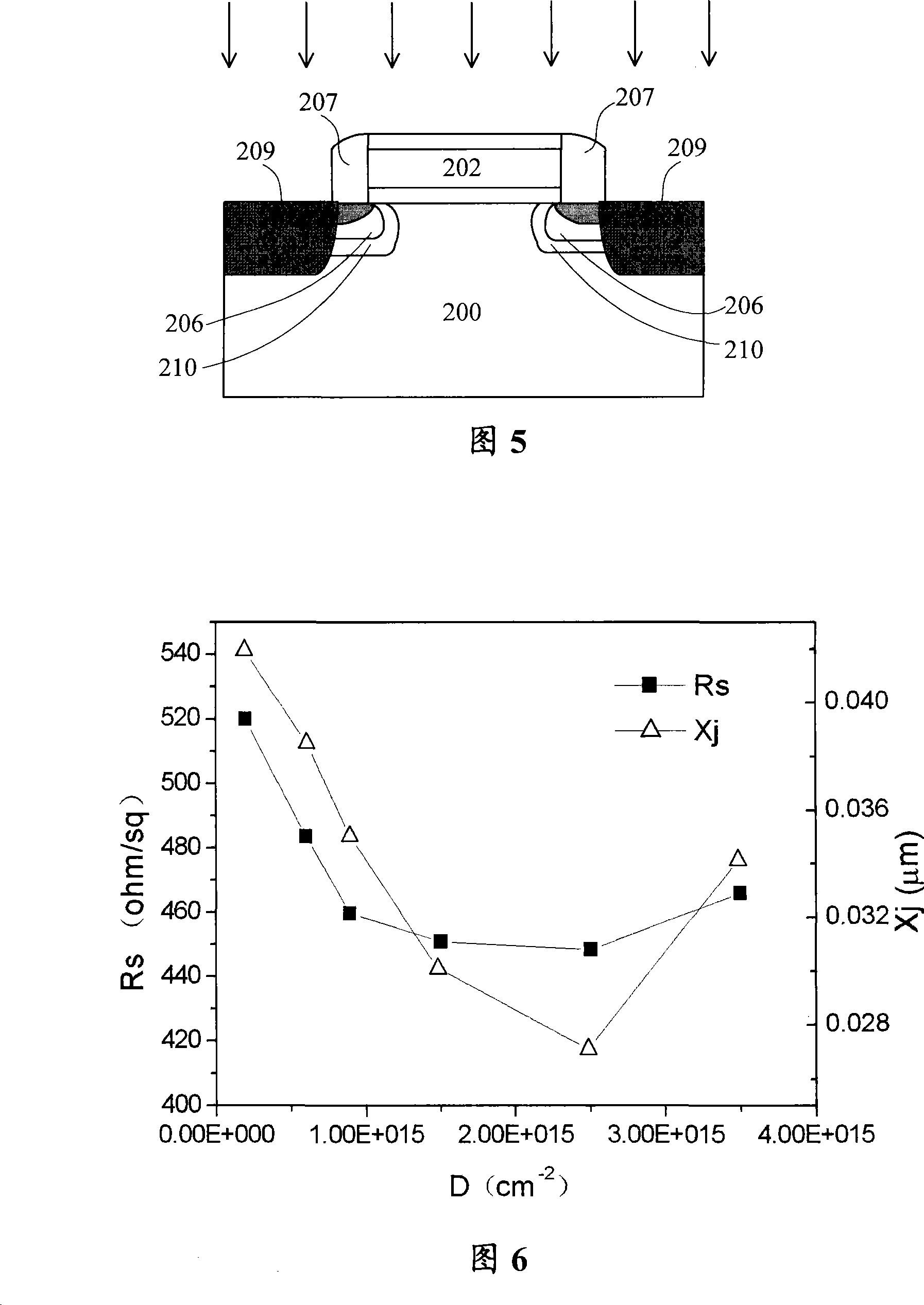
[0034] The present invention provides a MOS transistor, by doping F ions around the pocket region of the MOS transistor to form a F ion doped region, suppressing the transient enhanced diffusion effect of doping ions in the pocket region, and reducing the junction leakage of the MOS transistor current, improving the performance of MOS transistors.

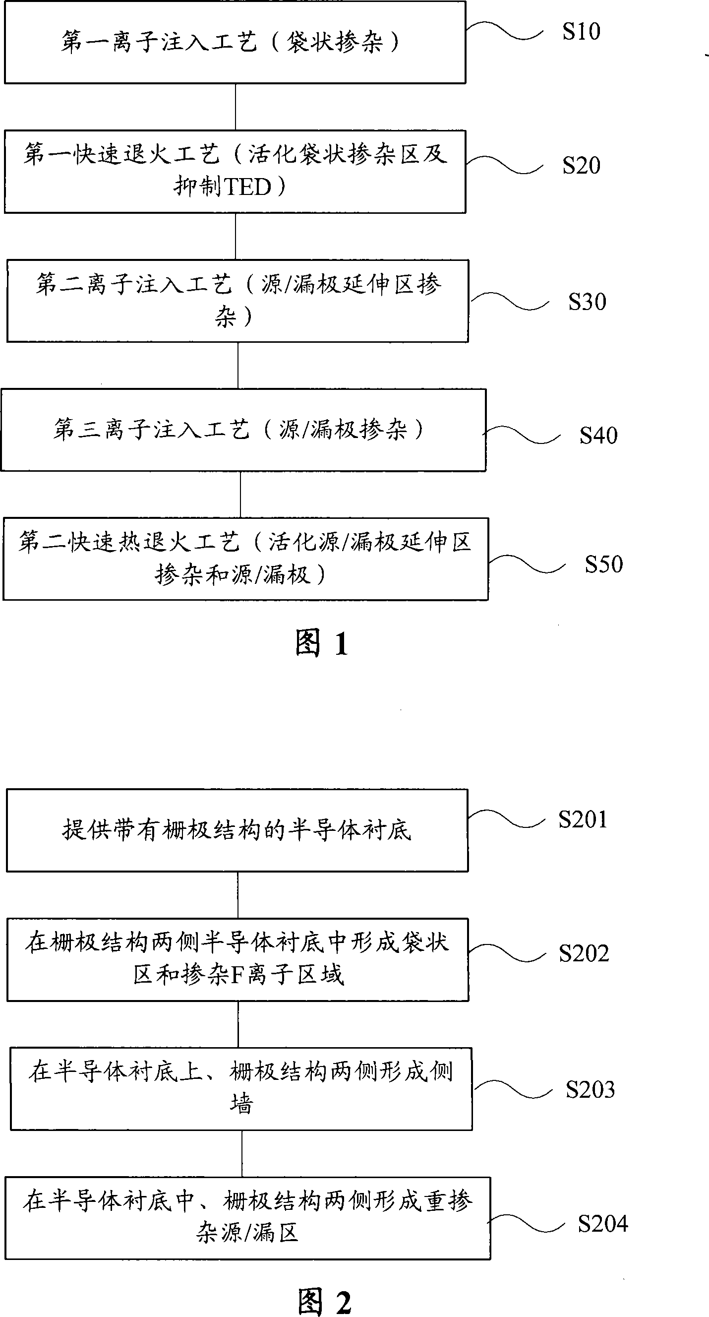
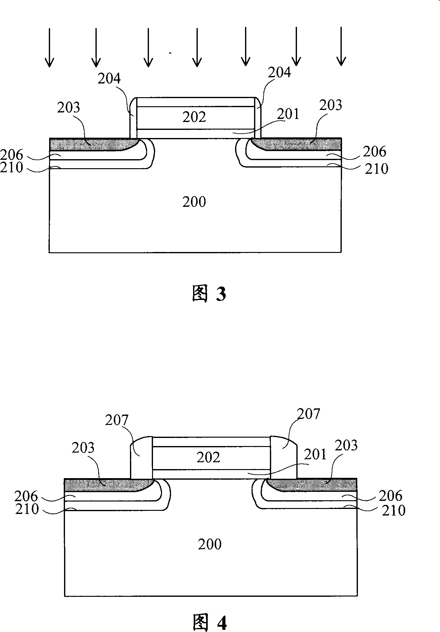
[0035] refer to figure 2 It is a schematic flow chart of a specific embodiment of forming a MOS transistor in the present invention, including the following steps: performing step S201, providing a semiconductor substrate with a gate structure; performing step S202, forming pockets in the semiconductor substrate on both sides of the gate structure Shaped region and doped F ion region, the doped F ion region is located around the pocket region; step S203 is performed to form sidewalls on the semiconductor substrates on both sides of the gate structure; step S204 is performed to form sidewalls on both sides of the gate structure A ...


PUM


Abstract

An MOS transistor comprises low doped source / drain extended regions in a semiconductor substrate and on two sides of a grid structure, sidewalls located on the semiconductor substrate on two sides of the grid structure, heavily doped source / drain regions located in the semiconductor and on two sides of the grid structure, and pocket regions and F-ion doped regions respectively located in the semiconductor substrate and on two sides of the grid structure, wherein the F-ion doped regions are located around the pocket regions. The invention further provides a method of forming the MOS transistors. By forming the F-ion doped regions around the pocket regions of the MOS transistor, transient enhanced diffusion effect of ions from the pocket regions into the semiconductor substrate can be prevented, thereby reducing junction depth, decreasing junction current leakage, and improving the performance of the MOS transistor.

Description

technical field [0001] The invention relates to the field of semiconductors, in particular to a MOS transistor with a pocket region and a forming method thereof. Background technique [0002] Pockets (halo) are typically formed in metal-oxide-semiconductor transistor (MOSFET) devices with channel lengths below 0.18 μm. The shrinking of the channel length between the source / drain leads to undesired punch through current due to the close proximity of the source / drain depletion regions. An effective method to prevent punch through current is to form a pocket (pocket / halo) around the source / drain. The conductivity type of these regions is the same as that of the semiconductor substrate or the doped well forming the MOSFET region, but its doping concentration is higher than that of the semiconductor substrate or the doped well, which is different from the MOSFET without the pocket region. Ratio, the degree of depletion of the depletion region can be reduced, thus resulting in a...

Claims


Application Information

Patent Timeline
Patent Type & Authority Patents(China)
IPC IPC(8): H01L21/336H01L29/78H01L29/06
Inventor 赵猛
Owner SEMICON MFG INT (SHANGHAI) CORP
Why Eureka
Try Eureka