Chip fixing device for finding chip defect by luminous microscope

A fixed device, a technology under the microscope, applied in the direction of optical testing flaws/defects, measuring leads/probes, etc., can solve the problems of waste of cost, poor versatility, difficult to control, etc., to achieve good applicability, stable center of gravity, and avoid clutter. Effect

Inactive Publication Date: 2008-12-10
SEMICON MFG INT (SHANGHAI) CORP +1
View PDF5 Cites 0 Cited by
  • Summary
  • Abstract
  • Description
  • Claims
  • Application Information

AI Technical Summary

Problems solved by technology

[0003] With the rapid development of the speed and integration of silicon chips, the metal layer on a chip has reached up to 8 layers. Because these metals block the light, EMMI cannot detect the light emitted by the defect from the front of the chip, thus developing from The technology of detecting defects on the back of the chip, however, the traditional method is to use a complex special tool to dig out a window of a specific size on the back of the chip, remove the package plastic, lead frame, etc., then polish the back, and put the chip Place it in a special-sized card slot, and then search for defects...During this process, digging the window is an extremely time-consuming and difficult to control work, and each commercially available card slot can only be used for one size Chips with low versatility will cause a waste of cost, and it will take a few days to find only one defect! really should be improved

Method used


Image

  • Chip fixing device for finding chip defect by luminous microscope
  • Chip fixing device for finding chip defect by luminous microscope
  • Chip fixing device for finding chip defect by luminous microscope

Examples


Embodiment Construction

[0011] The present invention will be described in detail below through specific examples.

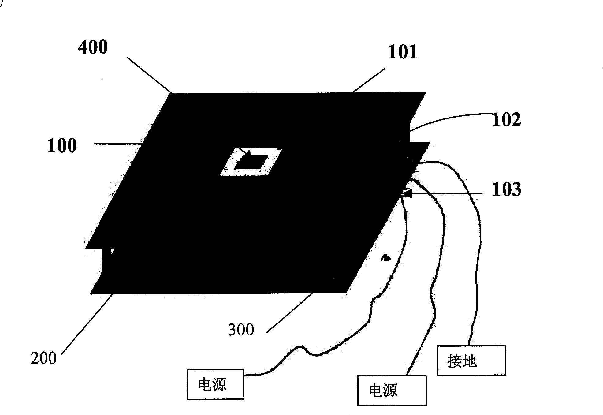
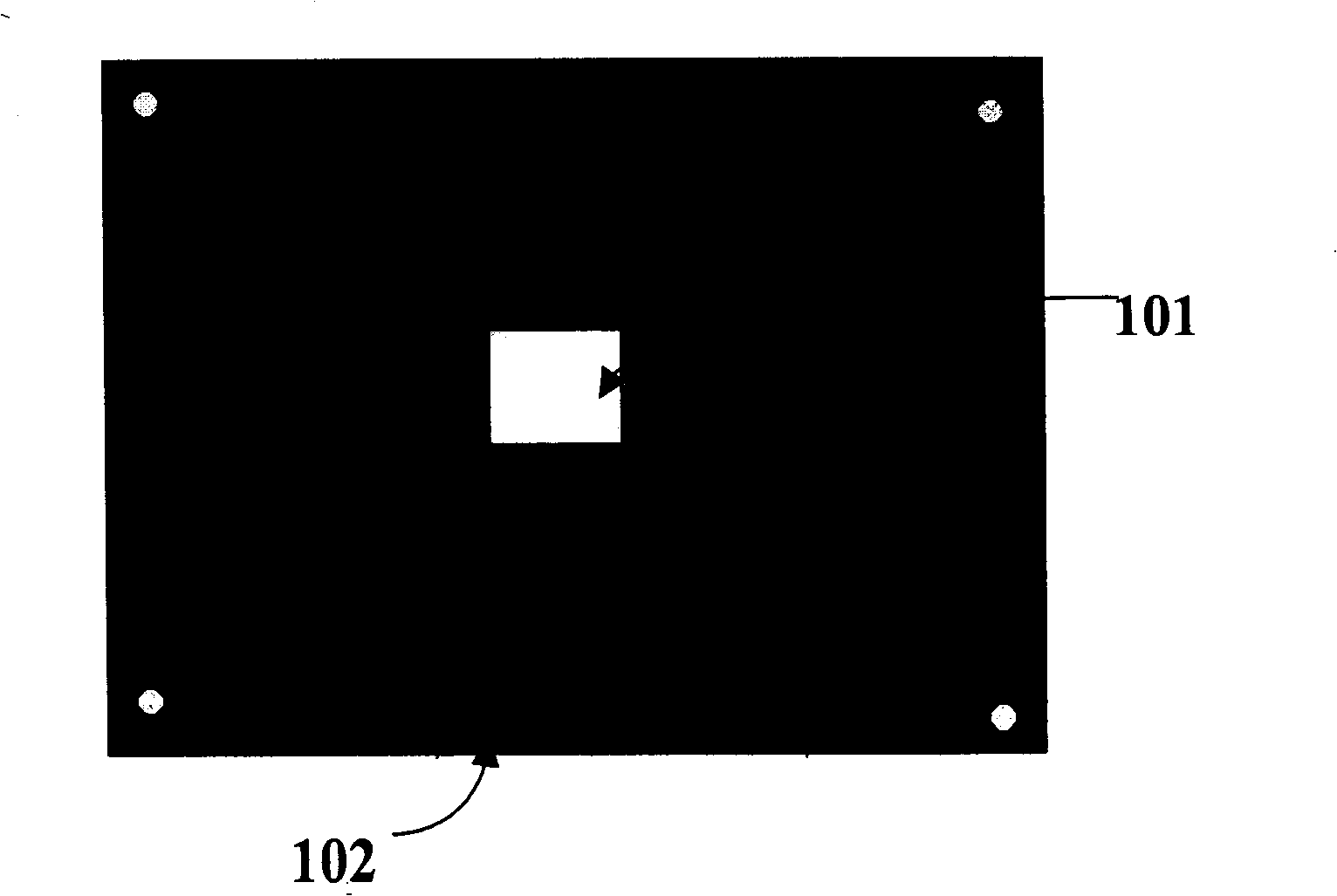
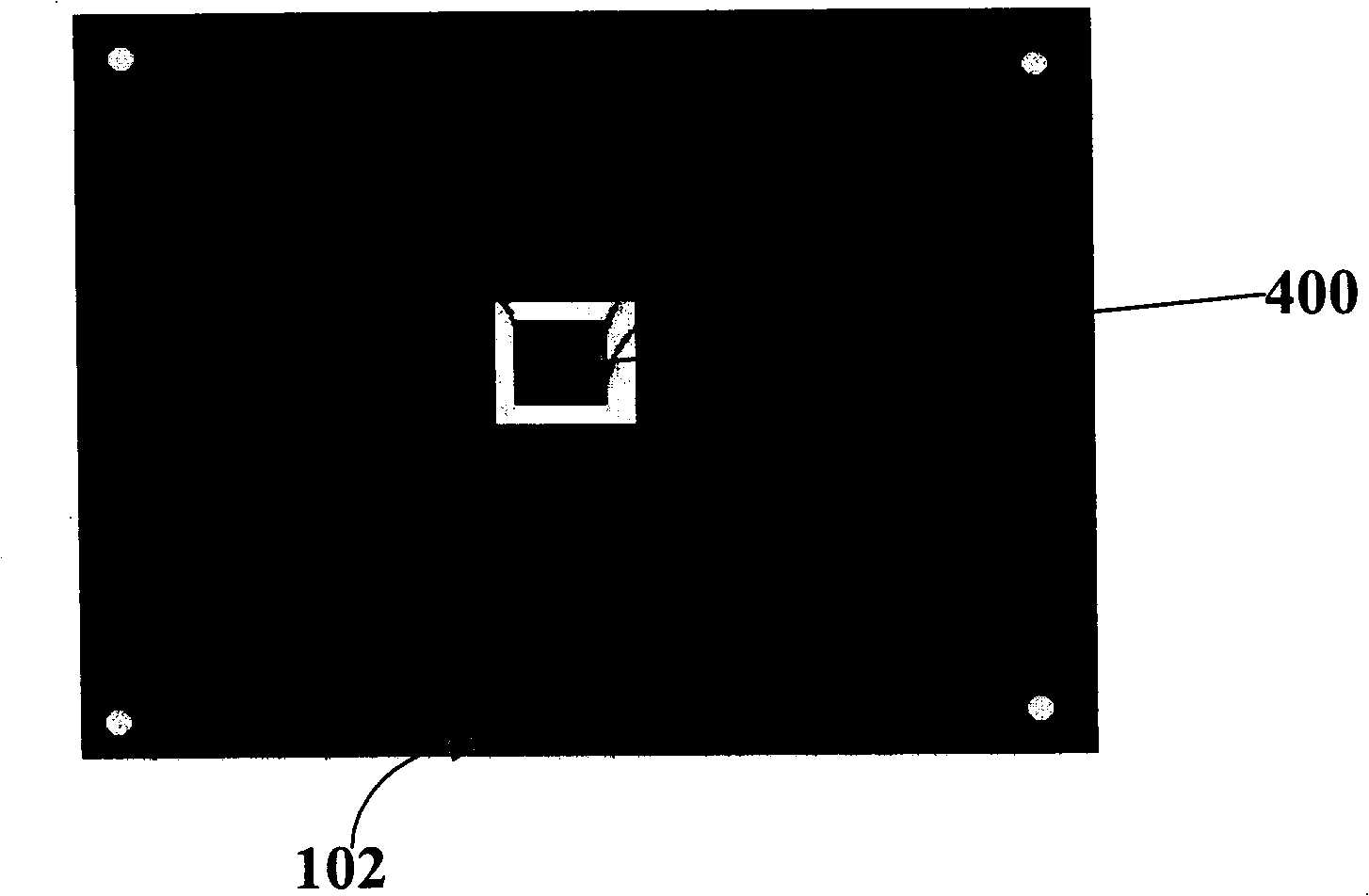
[0012] please see figure 1 As shown, it is a schematic diagram of the fixing device of the present invention. In this embodiment, the fixing device is a structure comprising upper and lower layers, the upper layer is a printed circuit board (PCB board) 100; the lower layer is a fixing plate 200 for fixing , made of heavier materials such as stainless steel, etc., so that the center of gravity of the fixing device remains relatively stable, and the chip can be stably presented under the lens of the light-emitting microscope during operation; and this two-layer structure makes it easy to The upper printed circuit board avoids the trouble of being entangled by electrical wires; the printed circuit board 100 and the fixing plate 200 are thus figure 1 The rectangle, also can be other shapes, is provided with support element 300 between the two, figure 1 The middle support element 300 is fo...


PUM


Abstract

This invention relates to a chip fixing device used in emission microscope to find out chip defection, which comprises the following parts: one printing circuit with multiple electrically connected lines to provide power to chips fixed on the observation window; one observation window made of transparent materials located on the printing circuit board; one fixing board located on the down layer of the printing circuit board. The multiple connection lines are printed around observation window and are isolated between each other to supply power to the chip. Each connection line is located with one line terminal around the printing circuit board edge.

Description

technical field [0001] The invention relates to the technical field of semiconductor manufacturing, in particular to a chip fixing device used for an emission microscope (emission microscope, EMMI) to find chip defects. Background technique [0002] In the semiconductor industry, functional testing of packaged semiconductor chips is an essential technology to improve the yield of chips. Among them, the light-emitting microscope is an important tool for finding the defect position on the integrated circuit. The principle is: When a voltage is applied to the chip, when there is a defect in a certain component of the chip, the defect will emit abnormal infrared light radiation. The light-emitting microscope uses this abnormal infrared light radiation to find the exact location of the defect on the chip. position, and then the failure analysis engineer (failure analysis engineer) can conduct further research on the chip to find out the root cause, thereby improving the final yie...

Claims


Application Information

Patent Timeline
Patent Type & Authority Patents(China)
IPC IPC(8): G01R1/06G01N21/88
Inventor 董伟淳廖炳隆季春葵牛崇实
Owner SEMICON MFG INT (SHANGHAI) CORP
Why Eureka
Try Eureka