Organic electroluminescence device

An electroluminescence device and luminescence technology, applied in the direction of electroluminescence light source, electric solid-state device, electric light source, etc., can solve the problems of upper limit of device operating temperature, influence of device stability, low glass transition temperature, etc., and achieve improvement Good production efficiency, good stability and high luminous efficiency

Active Publication Date: 2008-12-31
BEIJING VISIONOX TECH
View PDF6 Cites 0 Cited by
  • Summary
  • Abstract
  • Description
  • Claims
  • Application Information

AI Technical Summary

Problems solved by technology

However, compared with electron transport materials, hole transport materials have poor stability due to their lower glass transition temperature, which affects the stability of the device, and the upper limit of the operating temperature of the device is also greatly limited.

Method used


Image

  • Organic electroluminescence device
  • Organic electroluminescence device
  • Organic electroluminescence device

Examples


Embodiment 1-4

[0030] Embodiment 1-4 (device number OLED1-4)

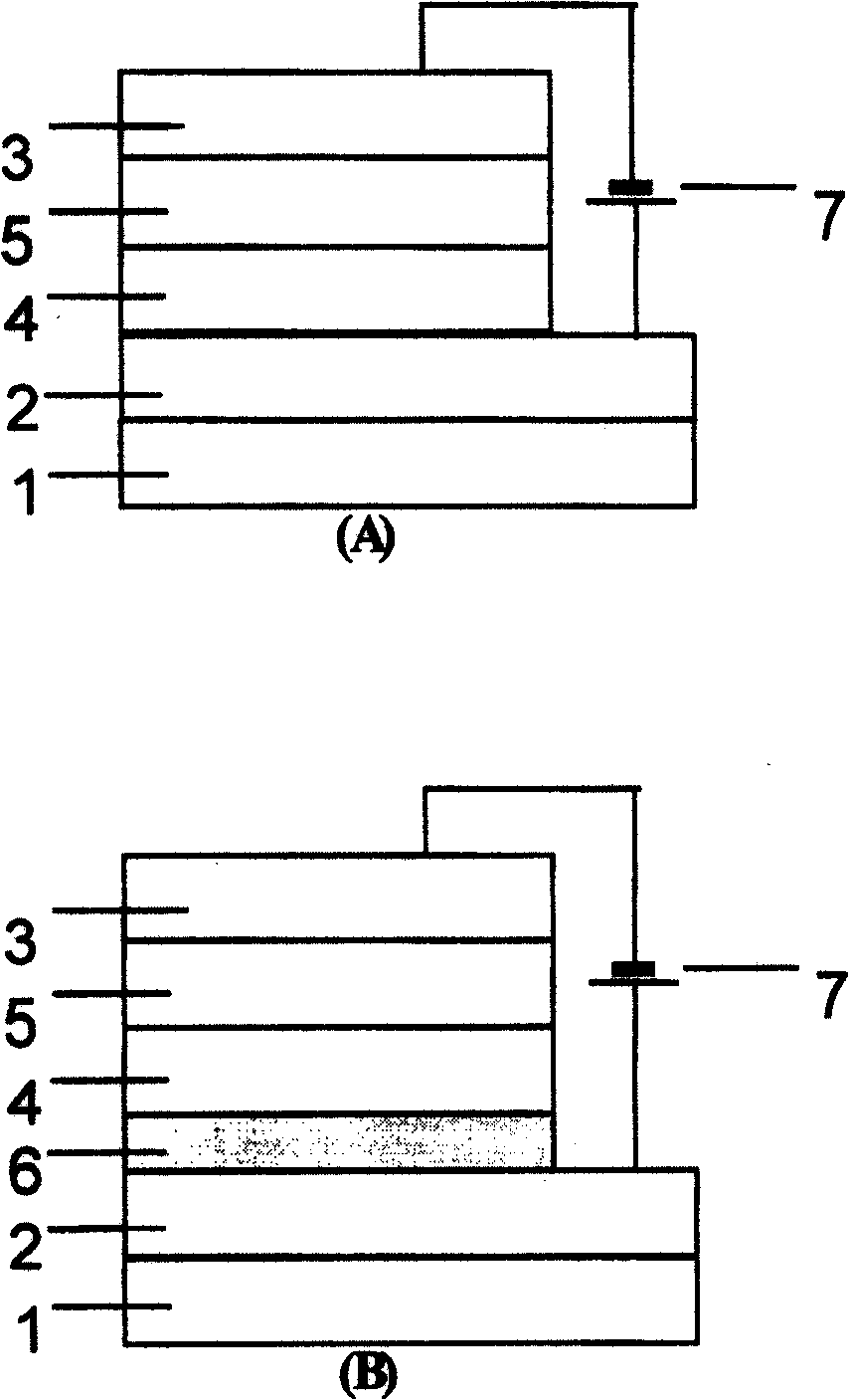
[0031] Glass / anode / Alq 3 :DMQA / BAlq / LiF / Al (1)

[0032] Four organic electroluminescence devices having the above structural formula (1) were prepared, and the anodes of these four devices used different electrode materials. The specific preparation method is as follows:

[0033] ① Clean the glass substrate by using boiling detergent ultrasonic and deionized water ultrasonic method, and place it under the infrared lamp to dry, and evaporate a layer of anode material on the glass with a film thickness of 80-280nm;

[0034] ②Place the above-mentioned glass substrate with anode in a vacuum chamber, and evacuate to 1×10 -5 ~9×10 -3 On the anode layer film of Pa, continue to vapor-deposit a layer of Alq3 doped with DMQA as the organic light-emitting layer of the device, and use a dual-source vapor deposition method for doping. The ratio of the vapor deposition rate of Alq3 and DMQA is 10000: 1~ 100:2, the doping concentration of ...

Embodiment 5-7

[0040] Embodiment 5-7 (device number OLED5-7)

[0041] Glass / ITO / Teflon / Alq 3 :DMQA / Balq / LiF / Al (2)

[0042] Prepare 3 organic electroluminescent devices with the above structural formula (2), the specific steps of preparation are as follows:

[0043] ① Clean the ITO glass with a transparent conductive substrate with an anode by using boiling detergent ultrasonic and deionized water ultrasonic method, and place it under an infrared lamp for drying, in which the ITO film on the conductive substrate is used as the anode layer of the device , the sheet resistance of the ITO film is 5Ω~100Ω, and the film thickness is 80~280nm;

[0044] ②Put the above-mentioned cleaned and dried ITO glass in a vacuum chamber and vacuumize to 1×10 -5 ~9×10 -3 For Pa, a layer of Teflon is evaporated on the above ITO film as the hole injection layer of the device, the evaporation rate of the film is 0.01-0.2nm / s, and the film thickness is 0.5-20nm;

[0045] ③Continue to vapor-deposit a layer of A...

Embodiment 8-11

[0058] Embodiment 8-11 (device number OLED8-11)

[0059] Double-layer devices OLED8, OLED9, OLED10 and OLED11 were prepared by the same method as in Examples 5-7, and the electrodes of these four devices used different electrode materials from those in Examples 5-7. The structures and properties of the four OLEDs are shown in Table 4 below:

[0060] Table 4

[0061]


PUM

PropertyMeasurementUnit
thicknessaaaaaaaaaa
current densityaaaaaaaaaa

Abstract

The device consists of a substrate, an anode layer, an organic functional layer and a cathode layer. The organic layer contains a light emission layer and an electronic transport and holes barrier layer. The anode layer contains an electrode layer and anj anode modification layer, the anode modification layer contains a holes injection layer, the holes injection layer adopts the polymeric material that is prepared into an uniform distribution nanostructure on surface of film, and the inorganic insulation material.

Description

technical field [0001] The invention relates to an organic electroluminescent device, more specifically, to a double-layer organic electroluminescent device with high luminous efficiency and good stability. Background technique [0002] Today, with the development of multimedia technology and the advent of the information society, the requirements for the performance of flat panel displays are getting higher and higher. In recent years, three new display technologies: plasma display, field emission display and organic electroluminescent display have made up for the shortcomings of cathode ray tubes and liquid crystal displays to a certain extent. Among them, organic electroluminescent displays have a series of advantages such as self-illumination, low-voltage DC drive, full curing, wide viewing angle, and rich colors. Low, its response speed can reach 1000 times that of liquid crystal display, but its manufacturing cost is lower than the liquid crystal display of the same r...

Claims


Application Information

Patent Timeline
Patent Type & Authority Patents(China)
IPC IPC(8): H01L51/50H05B33/22H05B33/12H05B33/14H05B33/26
Inventor 邱勇王立铎高裕弟王海峰
Owner BEIJING VISIONOX TECH
Why Eureka
Try Eureka