Wafer array apparatus and method for arraying wafer

A technology for arranging devices and arranging directions, which is applied to cleaning methods and utensils, chemical instruments and methods, and cleaning methods using liquids, etc., and can solve problems such as increasing devices, low output, and complex structures

Active Publication Date: 2009-01-07
K C TECH
View PDF9 Cites 0 Cited by
  • Summary
  • Abstract
  • Description
  • Claims
  • Application Information

AI Technical Summary

Problems solved by technology

[0017] As described above, the existing wafer alignment apparatus for mirror inversion has a very complicated structure, and the yield is low because mirror inversion is

Method used


Image

  • Wafer array apparatus and method for arraying wafer
  • Wafer array apparatus and method for arraying wafer
  • Wafer array apparatus and method for arraying wafer

Examples


Embodiment Construction

[0040] Hereinafter, embodiments of the present invention will be described in detail with reference to the drawings.

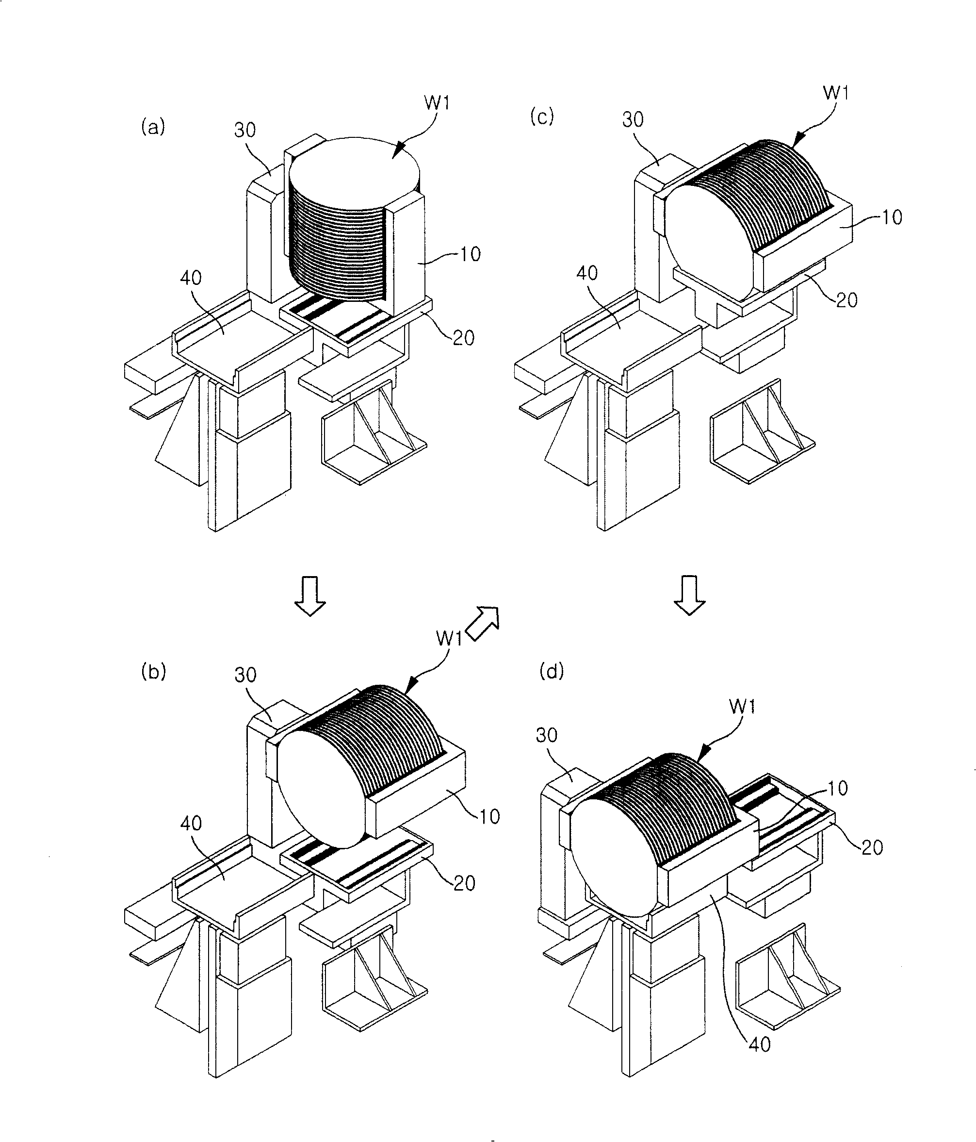
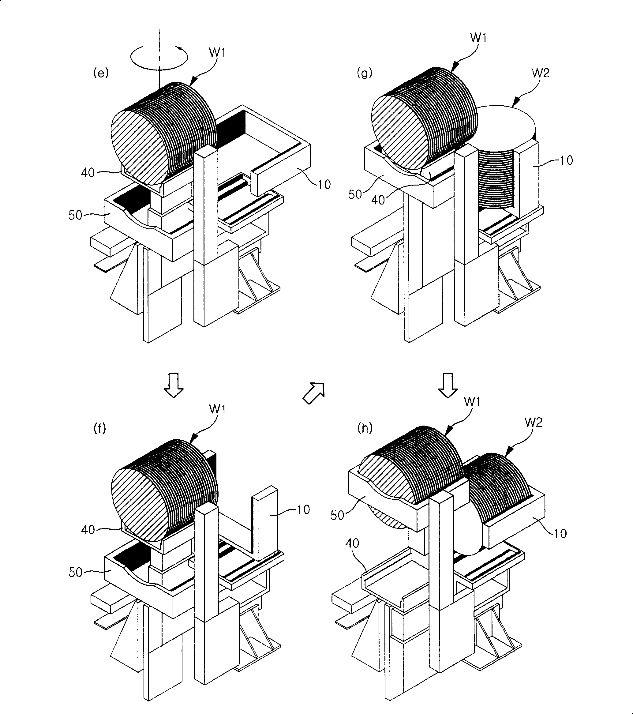
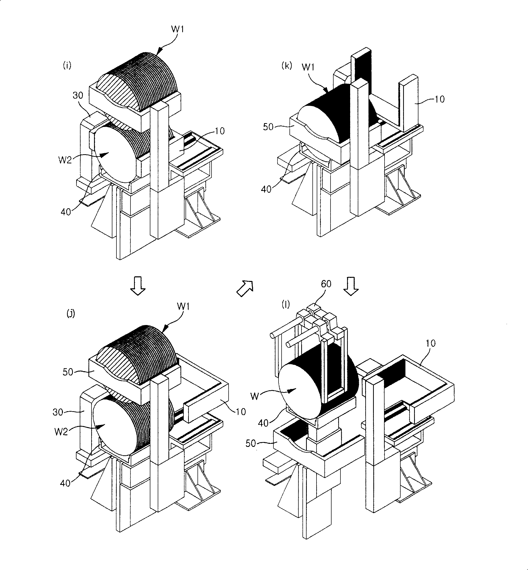
[0041] Figure 4 It is a side view of the first embodiment of the wafer alignment device provided by the present invention as a whole.

[0042] like Figure 4 As shown, the wafer alignment device provided by the present invention includes a wafer receiving unit 200 that rotates the wafer 90 degrees around the horizontal axis and a push unit 300 that rotates the wafer 180 degrees around the vertical axis. At this time, wafers are supplied from the robot 100 to the wafer receiving unit.

[0043] The robot 100 supplies a first wafer group and a second wafer group each composed of a plurality of wafers to the wafer receiving unit 200, respectively. At this time, the wafers of the first wafer group and the second wafer group are supplied to the wafer receiving unit 200 in a horizontal state.

[0044] Hereinafter, a case where the number of chips in each chip gr...


PUM


Abstract

The invention relates to a wafer array apparatus which makes opposite surfaces of a pair of adjacent wafers have a same property during a process of cleaning a plurality of wafers at one time by arraying wafers. The wafer array apparatus provided according to the invention includes a wafer receiving unit for receiving a first wafer group and a second wafer group composed of at least a wafer respectively in a horizontal state and arranging the wafer groups in a vertical state, and a delivering unit for orderly receiving the first wafer group and second wafer group of the vertical state and arranging the groups, and the wafer array apparatus further has a sturcture in which the wafers of the first wafer group and the second wafer group are alternately arrayed in opposite directions by the rotation of either the wafer receiving unit or the delivering unit.

Description

technical field [0001] The invention relates to a wafer arrangement device, in particular to a wafer arrangement device which makes the opposing surfaces of a pair of adjacent wafers have the same properties during the process of cleaning many wafers at one time by arranging the wafers. Background technique [0002] Generally, among the wafer cleaning methods used in the semiconductor manufacturing process, the wet cleaning method, which uses cleaning liquid and deionized water to remove pollutants on the wafer surface, has a high throughput and can remove various pollutants at the same time, and can be carried out Batch cleaning has therefore become the most widely used cleaning method in semiconductor manufacturing processes. [0003] Generally, a cleaning device used in a wet cleaning method is mainly composed of a carrying-in unit, a cleaning treatment unit, and a carrying-out unit. The carrying-in section includes a placement table for receiving wafers from a wafer car...

Claims


Application Information

Patent Timeline
IPC IPC(8): H01L21/677H01L21/67H01L21/30H01L21/00B65G49/00B65G47/74B08B11/00B08B3/04
CPCH01L21/67057H01L21/67718H01L21/67745H01L21/68Y10S414/136
Inventor 姜炳州孙永成赵显佑李泰雨朴美爱
Owner K C TECH
Why Eureka
Try Eureka