Positioning assembling device for contact pin tinning process and contact pin tinning method

A technology for positioning tooling and pins, applied in the direction of assembling printed circuits with electrical components, etc., can solve the problems of inaccurate pin size, long production cycle, increased cost of tinning process, etc., to eliminate waiting for turnover and storage. The effect of saving equipment and space and improving product quality

Inactive Publication Date: 2009-01-21
广州博士科技交流中心有限公司
View PDF5 Cites 0 Cited by
  • Summary
  • Abstract
  • Description
  • Claims
  • Application Information

AI Technical Summary

Problems solved by technology

[0004] 1) After the pin is inserted into the circuit board, it is easy to tilt without auxiliary fixing, resulting in the pin being not perpendicular to the circuit board after welding;
[0005] 2) Due to the buoyancy of the tin and the heat deformation of the single board when passing the tin, it is easy to make the pins float, resulting in inaccurate dimensions of the pins in the height direction, and easy to form virtual soldering
[0015] (1) The production cycle is long and the work efficiency is low: because the tinning process requires the process of dispensing red glue, and because the red glue takes a long time to cure, the circuit board needs to be removed from the production line, etc., which will result in time-consuming, affect the rhythm of the production line, and damage Disadvantages of process balance;
[0016] (2) Due to the use

Method used


Image

  • Positioning assembling device for contact pin tinning process and contact pin tinning method
  • Positioning assembling device for contact pin tinning process and contact pin tinning method
  • Positioning assembling device for contact pin tinning process and contact pin tinning method

Examples


Embodiment Construction

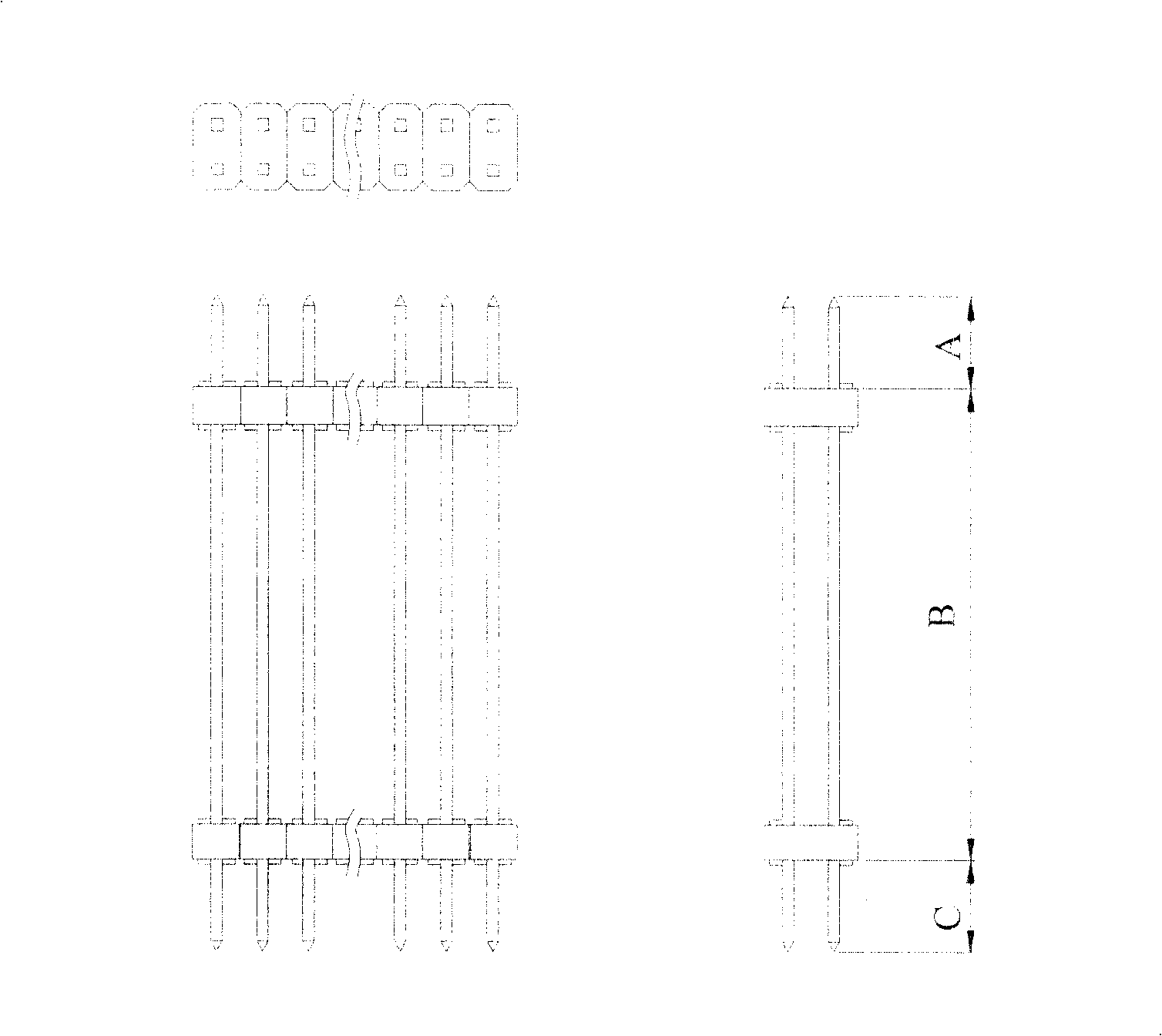
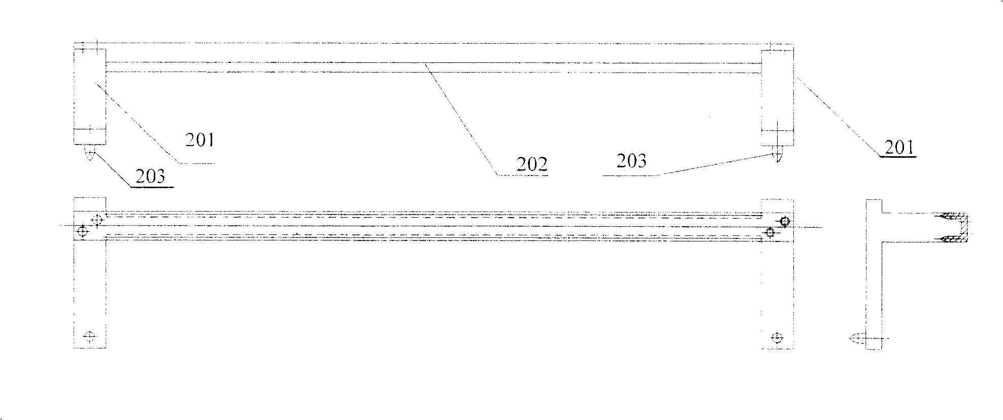
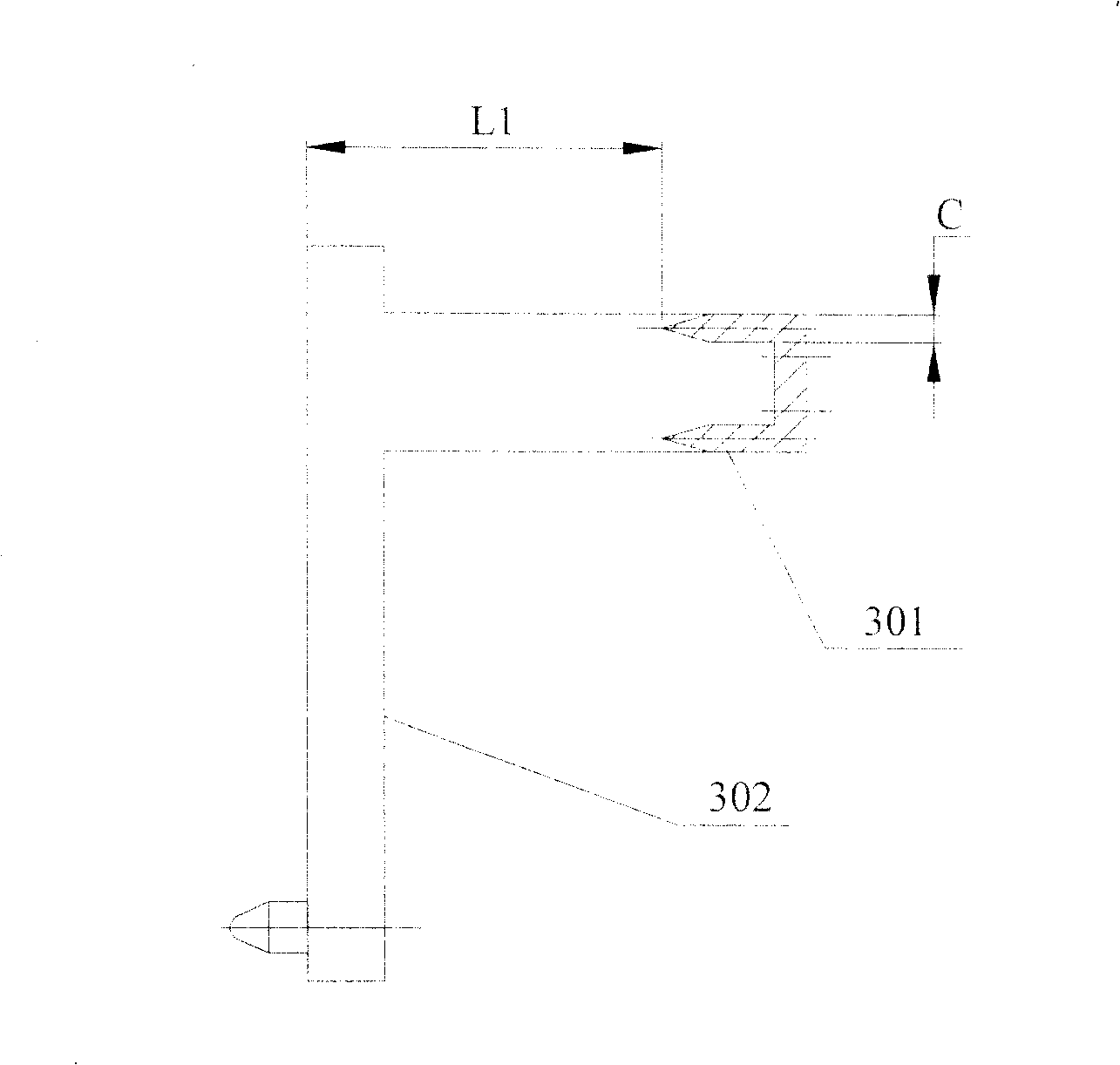
[0054] The present invention relates to a positioning tooling device in the tinning process of inserting pins and a tinning method using the device. The positioning tooling device is composed of a bracket, a positioning pin and a guiding rod, and the guiding part on the guiding rod Realize the positive guiding effect on the pins, so as to ensure the dimensional accuracy of the pins in the process of tin passing. When using this positioning tool to carry out soldering of pins, after inserting the pins into the circuit board, use the positioning tool to act on the pins to guide the pins so that the pins meet the positioning requirements in size, and then, in the Under the action of the positioning tool, the pins are tinned.

[0055] The present invention will be described in detail below in conjunction with the accompanying drawings.

[0056] In order to realize the tin-passing process of pins on the circuit board, the present invention adopts figure 2 Tooling shown complete ...


PUM


Abstract

The invention discloses a locating industrial mounting device in a pin soldering process, and the device includes: straight leader, brackets and locating pin, where two ends of the straight leader are connected vertically with the brackets, respectively, the distance tolerance between the acting height of a straight leading part in the straight leader and a pin plastic pad is between 0 and a preset tolerance, and the difference value between the pin-pin distance and the width of the straight leading part is between o and a corresponding preset tolerance. The invention also discloses a pin soldering method using the locating industrial mounting device, including the following steps: firstly, inserting pins in a circuit board, inserting the locating industrial mounting device on the circuit board by the locating pin to make the leading part of the straight leader act on the pins; and then making pin soldering.

Description

technical field [0001] The invention relates to the field of circuit board processing, in particular to the field of tin-passing technology for pins on the circuit board. Background technique [0002] The pin is an electronic component widely used on the circuit board. The pin has a variety of specifications, including connector type, patch type, single row, double row, multi-row, and according to different needs, the pin The size will also vary. This article is for connector-type pins. Its structure is like figure 1 shown. exist figure 1 In the illustrated pin structure, the pins are composed of a plurality of identical units, and the number of combined units of the pins and the number of rows of pins in each combined unit can vary according to actual needs. In the process of circuit board processing, a tinning process is required, which is also called reflow soldering, which is a process in which components inserted on the circuit board are soldered to the circuit boa...

Claims


Application Information

Patent Timeline
IPC IPC(8): H05K3/34
Inventor 张忠学
Owner 广州博士科技交流中心有限公司
Why Eureka
Try Eureka