
Flash storage cell structure and its preparation method

A flash memory storage and deposition technology, used in electrical components, semiconductor/solid-state device manufacturing, semiconductor devices, etc., can solve the problems affecting the reading of stored data, improve storage density, crosstalk, etc., to reduce storage costs and increase storage density. , the effect of suppressing the effect of crosstalk

Active Publication Date: 2009-03-11
PEKING UNIV +1
View PDF2 Cites 0 Cited by
  • Summary
  • Abstract
  • Description
  • Claims
  • Application Information

AI Technical Summary

Problems solved by technology

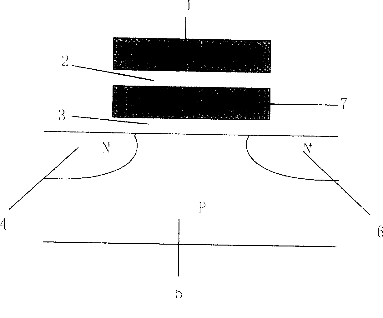
However, a problem with NROM is that the charges stored at both ends of the device have a horizontal distribution, so when the size of the device is reduced, there will be crosstalk between the two bits of data stored in NROM, which will affect the reading of the stored data, so it is difficult to further develop Improve storage density

Method used

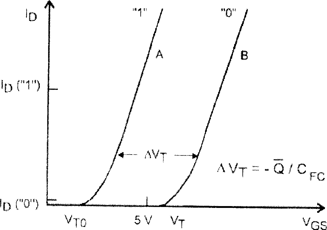
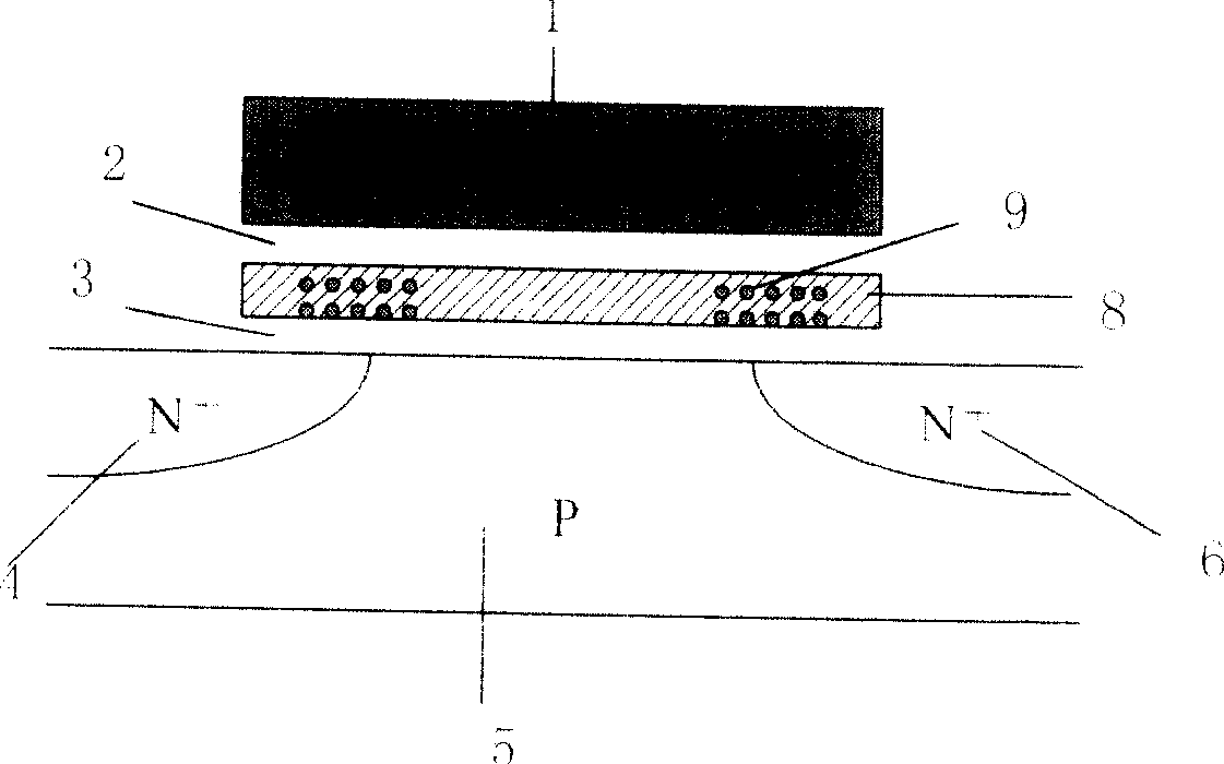

Image

  • Flash storage cell structure and its preparation method
  • Flash storage cell structure and its preparation method
  • Flash storage cell structure and its preparation method

Examples


Embodiment Construction

[0039] refer to Figure 5 , the unit uses two layers of silicon nitride 02 and silicon nitride 04 as the floating gate, and the floating gate is symmetrically located at both ends of the source and drain of the unit, the tunnel oxide layer 08 is 5-7nm, the first and second layers of nitrogen The thickness of the silicon carbide is 4-7 nm, the thickness of the oxide layer 03 between the two layers of silicon nitride is 2-3 nm, and the thickness of the blocking oxide layer 010 is 8-10 nm. Because the equivalent capacitance C of the first layer and the second layer of silicon nitride floating gate with respect to the control gate 01 FC Therefore, the electrons 09 stored in the two layers of floating gates make the threshold voltage shifts of the cells different. Taking the case of storing electrons at one end of the cell as an example, it is assumed that the equivalent capacitance of the first layer of silicon nitride relative to the control gate is C FC1 , and the electron cha...


PUM


Abstract

A flash storage cell is prepared as using two layers of silicon nitride as floating gate formed by close source region and drain region, storing two digit data separately on longitudinal direction and horizontal direction so as to realize four digit data storage function on each flash memory storage cell for greatly increasing storage density of flash memory.

Description

technical field [0001] The invention belongs to the technical field of non-volatile semiconductor memories, and in particular relates to a flash memory storage unit capable of storing multiple bits of data per unit and a preparation method thereof. Background technique [0002] Flash memory (Flash Memory) has become a research hotspot in non-volatile memory due to its convenience, high storage density and good reliability. Since the advent of the first flash memory product in the 1980s, with the development of technology and the demand for storage in various electronic products, flash memory has been widely used in mobile and communication devices such as mobile phones, notebooks, PDAs and U disks. . Today, flash memory has occupied most of the market share of non-volatile semiconductor memory, becoming the fastest growing non-volatile semiconductor memory. The development of flash memory with high storage density is an important driving force for the development of flash ...

Claims


Application Information

Patent Timeline
Patent Type & Authority Patents(China)
IPC IPC(8): H01L29/788H01L27/115H01L21/336H01L21/8247H10B69/00
Inventor 蔡一茂黄如单晓楠周发龙李炎王阳元
Owner PEKING UNIV
Learn More