Preparation method of fin channel dual-bar multi-functional field effect transistor

A field effect transistor and multifunctional technology, which is applied in the field of fin-channel double-gate multifunctional field effect transistor and its preparation, can solve the problem of affecting the DC characteristics and reliability of the device, long programming/erasing time, and affecting the reliability of the device. and other problems, to achieve the effect of improving programming/erasing speed, improving DC characteristics and reliability, and improving reliability

Active Publication Date: 2009-05-20
PEKING UNIV +1
View PDF5 Cites 0 Cited by
  • Summary
  • Abstract
  • Description
  • Claims
  • Application Information

AI Technical Summary

Problems solved by technology

[0006] However, the SOONO structure MOSFET multifunctional device shown in Document 1 is based on a planar double-gate device, and has the following problems: (1) The back gate ONO stack structure is too thick due to the device structure and manufacturing process (respectively 1.4nm, 42nm, 1.4nm, the total thickness reaches about 45nm), which makes the threshold window small (2.5V), the back gate voltage during programming / erasing is higher (up to 6V / -4V), and the programming / erasing time is longer (up to 0.5 ms / 0.5ms), the application of a thin tunnel oxide layer (1.4nm) makes the retention characteristics worse, and the too thick silicon nitride trap layer makes the redistribution of injected charges affect the reliability of the device; (2) tunnel oxidation The layer and the barrier oxide layer are prepared at the same time, so that they have the same thickness, and the thickness optimization design cannot be performed separately to improve the performance of the flash memory; (3) Compared with the conventional MOSFET preparation method, two layouts need to be added: a Stripe version (removing SiGe sacrificial layer), one is a deep trench isolation layout, which is used to isolate different back gates; (4) the back gate completely covers the channel and source and drain, and the band tunneling hot holes will be injected into the back gate during erasing The coverage area of ​​drain and drain affects the DC characteristics and reliability of the device
(5) The SiGe layer as the sacrificial layer and the silicon layer as the channel are both epitaxially grown, and the process cost is relatively high

Method used


Image

  • Preparation method of fin channel dual-bar multi-functional field effect transistor
  • Preparation method of fin channel dual-bar multi-functional field effect transistor
  • Preparation method of fin channel dual-bar multi-functional field effect transistor

Examples


Embodiment Construction

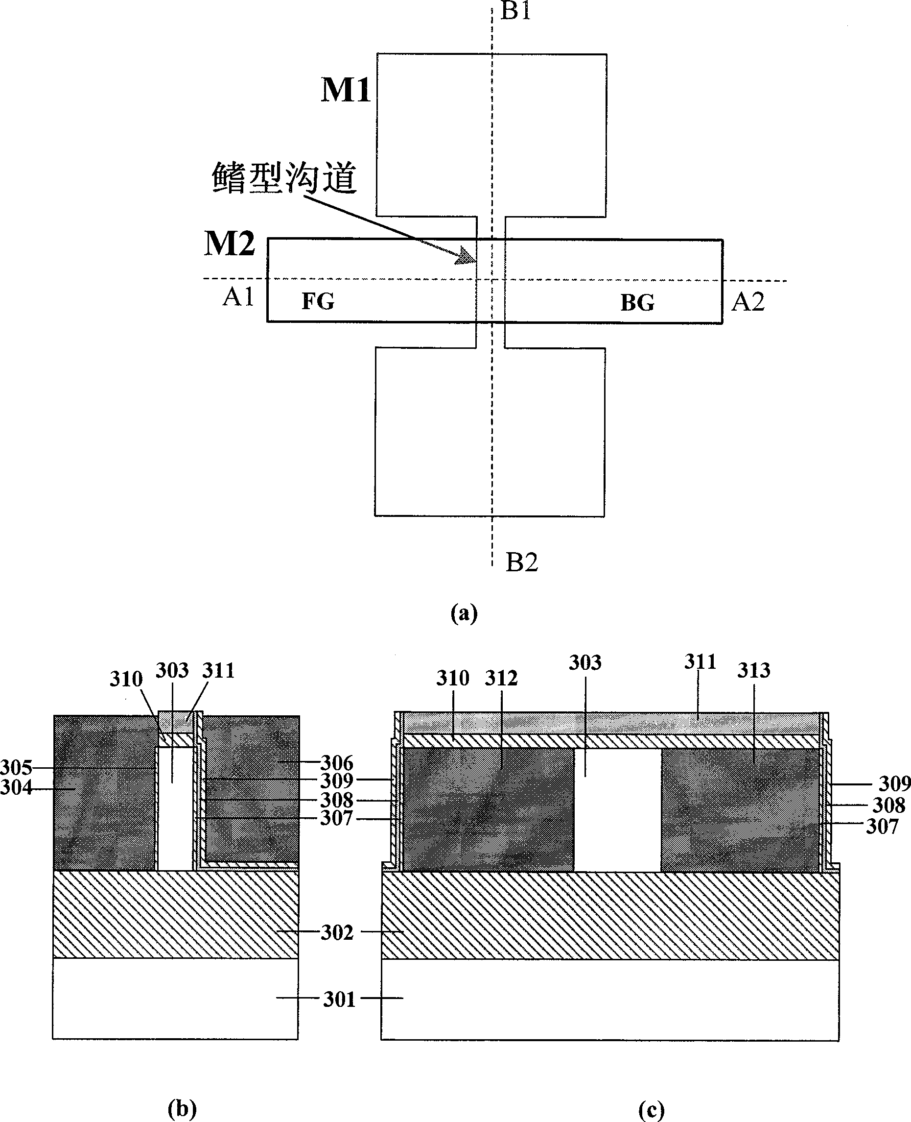
[0057] The fin channel dual-gate multifunctional field effect transistor provided by the present invention and its preparation method will be described in detail below in conjunction with the accompanying drawings, but this does not constitute a limitation to the present invention.

[0058] Such as image 3 Shown in (a)-(c) are the fin-type channel dual-gate multifunctional field effect transistors of this embodiment. The device is based on SOI substrate. Such as image 3 (a) shows the layout of the device, M1 is the active area version, and M2 is the gate version. Such as image 3 (b) and (c) are the cross-sectional structures of the device along the vertical direction of the channel (A1A2 direction) and along the channel direction (B1B2 direction), respectively. From the cross-sectional structure along the vertical direction of the channel, the field effect transistor is located on the silicon dioxide buried layer 302 of the SOI substrate, and the cross section of the ch...


PUM


Abstract

The invention provides a fin type channel dual-grid multifunctional field effect transistor and preparing method in metallic oxide semi-conductor field effect transistor technique field of the grand scale integration. The flied effect transistor is based on SOI underlay, the cross section of channel is rectangular fin along the vertical direction of the channel and forms the fin channel; a side of the channel is the grid oxide and the front grip, the other side is the tunnel oxide layer as the silicon nitride trap layer, the barrier oxide layer and the back grip of the charge storage layer and forms dual-grid structure; two edges of the fin channel are connected with the common n+ source and n+ leakage, the front grid aligns the back grid, the n+ source and the n+ leakage are covered less; the device achieves the channel section, the source section and the leakage section on the insulating layer based on SOI underlay. The invention is provided with high-effective MOSFET logical device function, the function of high-speed storage and the function of no condenser type DRAM.

Description

technical field [0001] The invention belongs to the technical field of metal oxide semiconductor field effect transistors (MetalOxide Semiconductor Field Effect Transistor—MOSFET) in ultra-large-scale integrated circuits (ULSI), and in particular relates to a fin-type channel double-gate multifunctional field-effect transistor and a preparation method thereof . Background technique [0002] With the wide application and high-speed development of VLSI, based on MOSFET, System On Chip (SOC) technology has aroused people's great interest more and more. The system chip integrates the units or modules that realize different functions in the whole system on one or as few integrated circuit chips as possible, so that each chip can realize multiple functions. SOC technology can overcome various problems in board-level integration of multi-chips (such as delay between chips, reliability of printed circuit boards), and has outstanding advantages in improving system performance, reduc...

Claims


Application Information

Patent Timeline
Patent Type & Authority Patents(China)
IPC IPC(8): H01L29/792H01L29/423H01L29/06H01L21/336H01L21/28
Inventor 吴大可周发龙黄如
Owner PEKING UNIV
Why Eureka
Try Eureka