Laminate, method of manufacturing the same, and method of manufacturing electronic component

a technology of laminate and electronic components, applied in the direction of solid-state devices, synthetic resin layered products, water-setting substance layered products, etc., can solve the problems of defective products, electronic components, and inability to easily remove gel from the substrate, and achieve excellent heat resistance, low elastic modulus, and low stress.

Inactive Publication Date: 2020-05-28
DOW TORAY CO LTD
View PDF0 Cites 4 Cited by
  • Summary
  • Abstract
  • Description
  • Claims
  • Application Information

AI Technical Summary

Benefits of technology

This patent describes a laminate that has a layer of silicone gel that is great at withstanding heat and has low elasticity, low stress, and excellent stress buffering properties. It is soft and flexible and can hold electronic components before and after curing. After curing, it becomes a hard layer that has better shape retention and mold-release properties. Using this laminate can help prevent issues like silicone gel deposits and defects in electronic components.

Problems solved by technology

However, since such a silicone gel is a “gel-form”, it is weak against deformation due to external stress such as vibration or internal stress due to expansion or contraction caused by temperature change, and in the case where the gel is destroyed or it is necessary to separate or cut (dice operation or the like) from an electronic member or the like requiring protection, adhesion or stress buffering, sticky deposits may remain on the object, or the gel may generate cohesive failure on the substrate, so that the gel cannot be easily removed from the substrate, the electronic component, or the like.
Such gel deposits are not preferable because they may cause defects in electronic components and the like, and also cause troubles and defective products during mounting of semiconductors and the like.
On the other hand, if the crosslink density of the organopolysiloxane is increased and completely cured, it is impossible to realize the properties of low elastic modulus, low stress, and excellent stress buffering properties which are the superiority of the silicone gel, and the followingness of the gel layer with respect to the uneven substrate is deteriorated, which may cause a gap and a separation from the substrate.
For this reason, conventional cured products such as silicone gel materials and silicone elastomers have not been able to solve the above-mentioned problems at all.
However, in the heretofore known curable compositions assuming multi-stage curing, there is no description or suggestion of the technical benefits of forming a silicone gel or changing from a soft gel to a hard completely cured product.

Method used


Image

  • Laminate, method of manufacturing the same, and method of manufacturing electronic component

Examples


examples

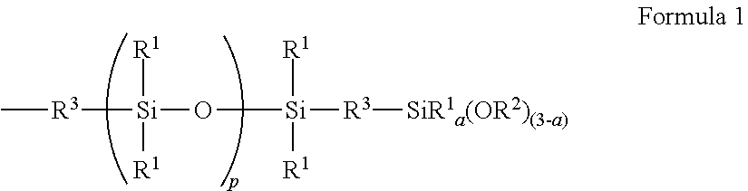
[0135]Hereinafter, the present invention will be described by way of examples, but the present invention is not limited thereto. In the examples shown below, the following compounds or compositions were used as raw materials.[0136]Component (A1-1): dimethylsiloxane polymer capped at both terminals with vinyldimethylsiloxy groups (polymerization degree of siloxane: about 540, vinyl group content: 0.13 weight %)[0137]Component (A1-2): dimethylsiloxane polymer capped at both terminals with vinyldimethylsiloxy groups (polymerization degree of siloxane: about 315, vinyl group content: 0.22 weight %)[0138]Component (A1-3): dimethylsiloxane / vinylmethylsiloxane copolymer capped at both terminals with trimethylsiloxy groups (polymerization degree of siloxane: about 1330, vinyl group content: about 0.47 weight %)[0139]Component (A2): resinous organopolysiloxane composed of trimethylsiloxy units (M units), vinyldimethylsiloxy units (MVi units), and Q units (vinyl group content: about 4.1 weigh...

examples 8 and 9

(2) Examples 8 and 9 and Comparative Examples 5 and 6

[0156]The liquid composition before curing was carried out at room temperature using a UV-irradiation device (MODEL UAW365-654-3030F, Centech, Inc.). In this case, a light source having a wavelength of 365 nm (about 40 mW / cm2) was used and irradiated twice for 90 seconds (the irradiation amount per unit area was 7200 mJ / cm2). At this time, in order to avoid contact between the high energy ray curable silicone composition and air, a PET film coated with a release agent and having a thickness of 50 microns was covered and irradiated with ultraviolet light. In Comparative Example 6, since there was no component (E2), a gel layer could not be prepared.

(3) Examples 10 to 12

[0157]The liquid composition before curing was left at room temperature for 1 hour to obtain a gel form.

Conditions for Manufacturing Secondarily Cured Products

examples 1 to 9

(1) Examples 1 to 9 and Comparative Examples 1 to 4 and 7

[0158]The curable gel layer was secondarily cured in nitrogen at 170° C. for 1 hour.


PUM

PropertyMeasurementUnit
Temperatureaaaaaaaaaa
Fractionaaaaaaaaaa

Abstract

Provided is a laminate having, on a substrate, a gel layer which is excellent in heat resistance, has low elastic modulus, low stress and is excellent in stress buffering properties and flexibility, is soft and excellent in holding property of electronic components before curing, and after curing, the gel layer is changed to a hard cured layer which is higher in shape retention and excellent in mold releasability than before curing, and a method for manufacturing the same. Also provided is a method for manufacturing an electronic component in which use of the laminate makes it difficult to cause problems such as deposits of silicone gel or a cured product thereof to a substrate or an electronic component, and makes it difficult to cause problems of defects or defective products of the electronic component. The laminate includes a curing reactive silicone gel layer on at least one type of substrate.

Description

TECHNICAL FIELD[0001]The present invention relates to a laminate including a substrate and a curing reactive silicone gel layer which changes in physical properties from a gel layer which is soft and excellent in holding property of electronic components and the like to a hard cured product layer, and a manufacturing method thereof. The present invention also provides a method of manufacturing an electronic component using the same.BACKGROUND ART[0002]Silicone gels can be obtained by curing reacting organopolysiloxanes having reactive functional groups so as to have low crosslink density, and are excellent in heat resistance, weather resistance, oil resistance, cold resistance, electrical insulation, and the like, and exhibit low elastic modulus, low stress, and excellent stress buffering properties because of being a gel form, unlike ordinary elastomer products, and are widely used for protecting damping materials for optical applications, in-vehicle electronic components, and cons...

Claims


Application Information

Patent Timeline
IPC IPC(8): B32B5/18B32B7/12B32B27/28B32B27/26B32B7/06H01L23/29
CPCB32B27/283B32B2266/124B32B7/12H01L23/296B32B7/06B32B27/26B32B2305/72B32B2457/00B32B5/18C09J183/04H01L23/29H01L23/31C09D183/04C08G77/12C08G77/20C08L83/04B32B27/38B32B27/34B32B2264/102B32B27/065B32B13/045B32B2264/104B32B2250/02B32B2266/12B32B2255/205B32B2307/732B32B15/18B32B9/046B32B21/047B32B27/36B32B27/365B32B27/304B32B27/286B32B9/005B32B2307/306B32B15/20B32B2255/06B32B2307/546B32B2307/748B32B27/285B32B27/16B32B15/046B32B27/42B32B27/302B32B2262/101C08K5/56C08L83/00Y10T428/26Y10T428/31663B32B2383/00
Inventor FUKUI, HIROSHITOYAMA, KYOKODOGEN, RYOTAUSHIO, YOSHITO
Owner DOW TORAY CO LTD
Why Eureka
Try Eureka