Chip package body

A chip packaging and chip technology, which is applied to semiconductor devices, electric solid-state devices, semiconductor/solid-state device components, etc., can solve the problem of low utilization rate of bearing space, inability to reduce, and shorten the distance between the chip package body 100 and the next-level electronic device and other problems to achieve the effect of high component configuration density

Active Publication Date: 2009-06-10
VIA TECH INC
View PDF4 Cites 0 Cited by
  • Summary
  • Abstract
  • Description
  • Claims
  • Application Information

AI Technical Summary

Problems solved by technology

However, in the known chip package 100, these chips 120 are all configured on one side of the integrated passive element layer 114, so the utilization rate of the carrying space of the carrier 110 is relatively low.
In addition, since these chips 120 are all disposed on one side of the integrated passive component layer 114, the height H of these solder balls 130 cannot be reduced to shorten the distance between the chip package 100 and the next-level electronic device.

Method used


Image

  • Chip package body
  • Chip package body
  • Chip package body

Examples


Embodiment Construction

[0014] In order to make the above-mentioned features and advantages of the present invention more comprehensible, a detailed description is given below of preferred embodiments in conjunction with the accompanying drawings.

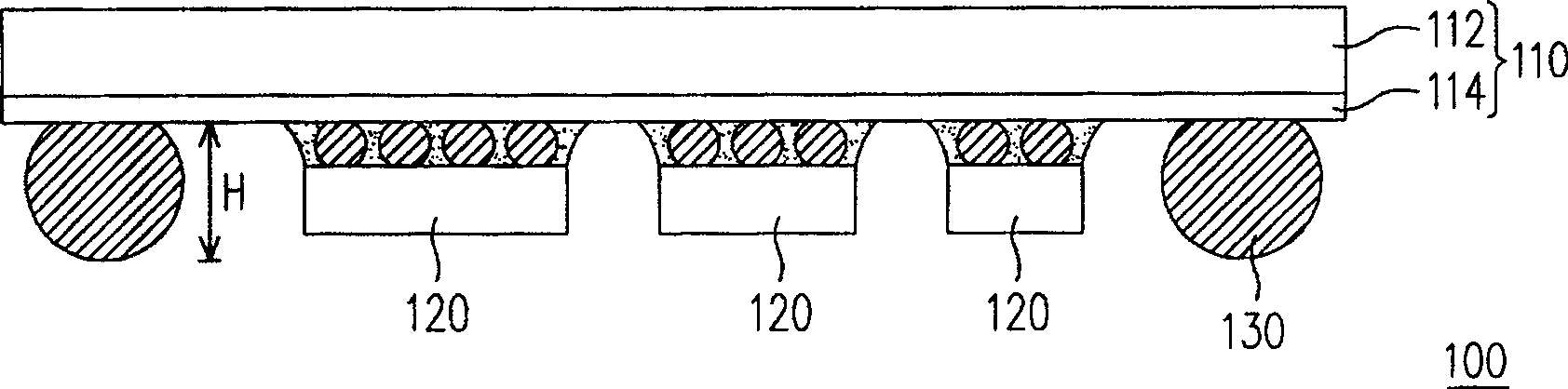
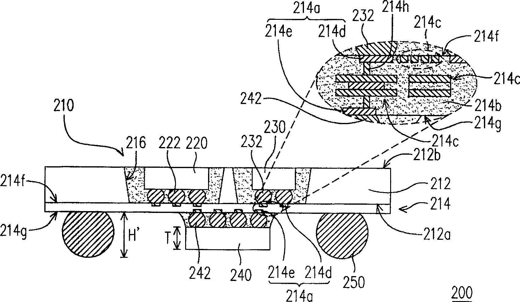
[0015] Please refer to figure 2 , Which shows a schematic side view of a chip package according to the first embodiment of the present invention. The chip package 200 includes a carrier 210 and a plurality of chips 220, 230, and 240. The carrier 210 includes a silicon substrate 212 and an integrated passive device layer 214. The silicon substrate 212 has two surfaces 212a and 212b opposite to each other. The integrated passive device layer 214 is disposed on the surface 212a. The chips 220, 230, and 240 are respectively disposed above the two opposite sides of the integrated passive device layer 214 and are electrically connected to the integrated passive device layer 214.

[0016] Since the chips 220, 230, and 240 are respectively disposed on opposite sides...


PUM


Abstract

This invention provides a chip package body including a loader, a silicon base plate and a first integration type passive element layer, in which, the silicon base plate includes a first surface and a second surface opposite to each other, the first conformity passive element layer is matched on the first surface and has a first pad group matched to the opposite two sides of the first integration passive element layer, in which, the density of the elements of the loader is high, and it's not necessary to add extra process devices to be integrated with the current process.

Description

Technical field [0001] The present invention relates to a chip package, and particularly relates to a chip package with an integrated passive device layer (IPD layer). Background technique [0002] In order to cope with the trend of light, thin, short, small, high-frequency, modular, and multifunctional electronic products, electronic components are relatively required to be more integrated and integrated. Therefore, the new era of high-frequency broadband materials and component technology will be the key to future technology. Through the breakthrough of new package materials, the development of new processes, and the integration of design technologies, the level of system in package (SIP) has now been reached. In addition, further develop high-frequency chip components, integrated passive device (IPD), micro-electro-mechanical system (MEMS) and nanomaterial technology to establish integrated module technology and improve high frequency Broadband product performance will be a wo...

Claims


Application Information

Patent Timeline
Patent Type & Authority Patents(China)
IPC IPC(8): H01L25/00H01L25/16H01L23/488
CPCH01L2224/10H01L2224/16227H01L2224/16235H01L2224/16265H01L2224/32225H01L2224/73204H01L2924/15156H01L2924/15311H01L2924/15321H01L2924/18161H01L2924/19011H01L2224/16225H01L2924/00
Inventor 蔡明霖
Owner VIA TECH INC
Why Eureka
Try Eureka