Memory device

A storage device and storage unit technology, applied in information storage, static memory, digital memory information, etc., can solve the problems of thermal deterioration of wiring, difficulty in realizing 3-dimensional capacitor array, and the need for polycrystallization, etc.

Inactive Publication Date: 2004-01-21
PANASONIC CORP
View PDF0 Cites 0 Cited by
  • Summary
  • Abstract
  • Description
  • Claims
  • Application Information

AI Technical Summary

Problems solved by technology

[0012] In order to suppress the occurrence of such a damaged region 116a, recovery annealing for recovering the damaged region 116a is performed after the formation of the ferroelectric capacitor 101, but the effect of completely disappearing the damaged region 116a is not effective.
[0013] In addition, since the recovery annealing treatment temperature is approximately the same as the temperature at which the ferroelectric film 116 is crystallized, when the ferroelectric capacitor 101 is multi-layered, recovery annealing is required for each layer, which causes the Thermal Deterioration of Wiring
Therefore, it becomes difficult to realize a three-dimensional capacitor array in which two or more layers of ferroelectric capacitors 101 are stacked.
[0014] In addition, the manufacturing method of the prior art, in Figure 7 In the process shown in (a), the ferroelectric film 116 is formed on the entire surface of the first electrode forming film 115A by the sputtering method or the sol-gel method, and polycrystallization is necessary.
Therefore, it will cause the average of the direction in which the polarization appears due to the isotropy of the crystal direction, so that it is very difficult to control the crystal direction of the ferroelectric to the direction in which the polarization deviation is maximized.

Method used


Image

  • Memory device
  • Memory device
  • Memory device

Examples


no. 1 Embodiment

[0046] A first embodiment of the present invention will be described below with reference to the drawings.

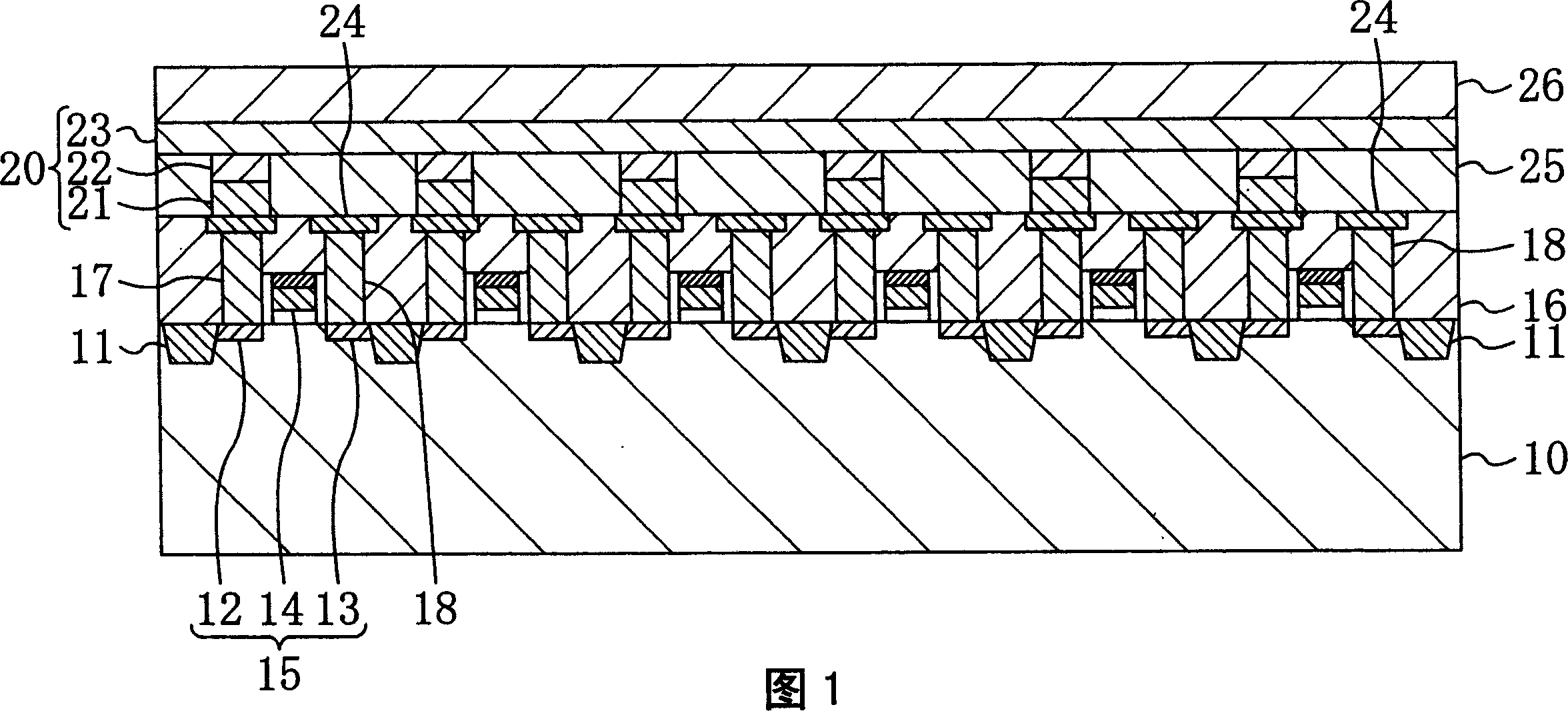
[0047] FIG. 1 is a cross-sectional view showing the structure of a memory cell array which is a main part of a memory device according to a first embodiment of the present invention.

[0048] As shown in FIG. 1 , a plurality of device regions divided by a plurality of device isolation regions 11 made of silicon oxide are formed on an upper portion of a semiconductor substrate 10 made of, for example, silicon. In each element region, a selection transistor 15 is formed as a switching element for selection. Each selection transistor 15 includes a source region 12 and a drain region 13 formed at intervals, and a gate 14 formed in a region between the source region 12 and the drain region 13 on the semiconductor substrate 10 .

[0049] The first insulating layer 16 is formed on the entire surface including each element isolation region 11 and each gate electrode 14 on the ...

no. 2 Embodiment

[0069] A second embodiment of the present invention will be described below with reference to the drawings.

[0070] 4 is a cross-sectional view showing the configuration of a memory cell array, which is a main part of a memory device according to a second embodiment of the present invention. In the second embodiment, the memory cell array is three-dimensional, that is, arranged by stacking two layers, so as to increase the arrangement density of the memory cells. In FIG. 4, the same components as those shown in FIG. 1 are denoted by the same reference numerals, and description thereof will be omitted here.

[0071] As shown in FIG. 4 , a peripheral circuit 40 including a selection transistor 15 , a first capacitor array layer 41 and a second capacitor array layer 42 in which a plurality of capacitors are arranged in an array are sequentially formed on a substrate 10 .

[0072] The first cell plate line 32A is formed after interposing the second insulating layer 31 between th...


PUM


Abstract

A memory device includes memory cells each having a capacitor including a lower electrode, a ferroelectric film and an upper electrode which are formed in this order over a substrate made of silicon. The ferroelectric film is selectively grown on the lower electrode. Such selective formation of the ferroelectric film on the lower electrode having a desired shape prevents a damaged portion from occurring in the ferroelectric film, thus making it possible to downsize the memory cells.

Description

technical field [0001] The present invention relates to a memory device including a capacitor using a capacitor film made of a ferroelectric in a memory cell. Background technique [0002] Figure 5 A conventional memory device is shown in which a memory cell is composed of a capacitor using a ferroelectric in a capacitor film and a selection transistor that can selectively access the capacitor. Such as Figure 5 As shown, one electrode of the ferroelectric capacitor 101 is connected to the source of the selection transistor 102, and the other electrode is connected to a cell plate line CP. The drain of the selection transistor 102 is connected to the bit line BL, and the gate is connected to the word line WL. [0003] An example of the cross-sectional configuration of a memory cell having such a circuit configuration is given in Figure 6 Indicated. Such as Figure 6 As shown, the selection transistor 102 is composed of: a drain region 111 and a source region 112 formed...

Claims


Application Information

Patent Timeline
Patent Type & Authority Applications(China)
IPC IPC(8): H01L27/105G11C11/22H01L21/02H01L21/316H01L21/8246H01L27/10H01L27/108H01L27/115
CPCH01L27/11507H01L21/31691H01L27/11502H01L28/55H01L21/02197H10B53/30H10B53/00
Inventor 嶋田恭博加藤刚久田中圭介上田大助
Owner PANASONIC CORP
Why Eureka
Try Eureka