Thin inductor embedded structure

A technology of inductive components and electronic components, which is applied in the directions of printed circuits connected with non-printed electrical components, transformer/reactor installation/support/suspension, etc. Problems such as inability to improve, to achieve the effects of easy processing and manufacturing, simplified structure, and improved production yield and production efficiency

Active Publication Date: 2018-09-28
鸿磬电子(东莞)有限公司
View PDF8 Cites 0 Cited by
  • Summary
  • Abstract
  • Description
  • Claims
  • Application Information

AI Technical Summary

Problems solved by technology

[0006] Furthermore, because the existing wire-wound inductors are all coils wound on the magnetic core, the wire-wound inductors do not have a planar structure for vacuum adsorption or clamping, so the existing wire-wound inductors can only The inductance element is welded on the circuit board by manual welding, but it is impossible to use automatic mechanical equipment to make the wire-wound inductor directly electrically connected to the circuit board, so it cannot be mass-produced, and it is welded by manual welding, and the alignment accuracy problem of bias
[0007] In particular, the coil 2 only has the middle section 14 of the magnetic core 1 for the wire to wind, and cannot wind all parts of the magnetic core 1, so the number of winding turns of the coil 2 will be limited, and the wire is openly arranged on the magnetic core, It also causes the inductance to be unable to increase, especially the existing SMD inductance components have a complex structure, which is not conducive to mass production and lower production costs

Method used


Image

  • Thin inductor embedded structure
  • Thin inductor embedded structure
  • Thin inductor embedded structure

Examples


Embodiment Construction

[0054] The embodiments of the present invention will be described in more detail below with reference to the drawings and reference numerals, so that those skilled in the art can implement them after studying this specification.

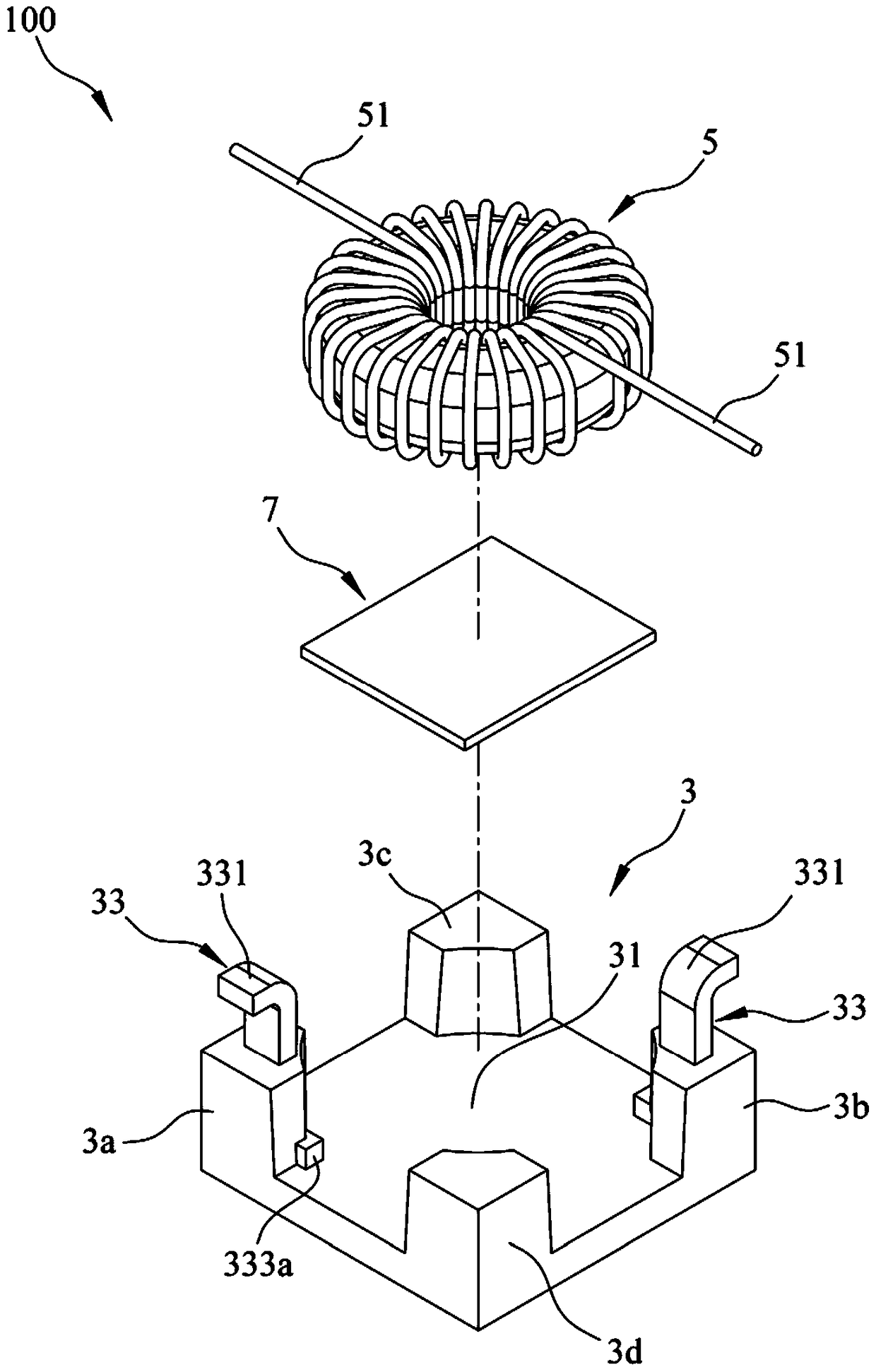
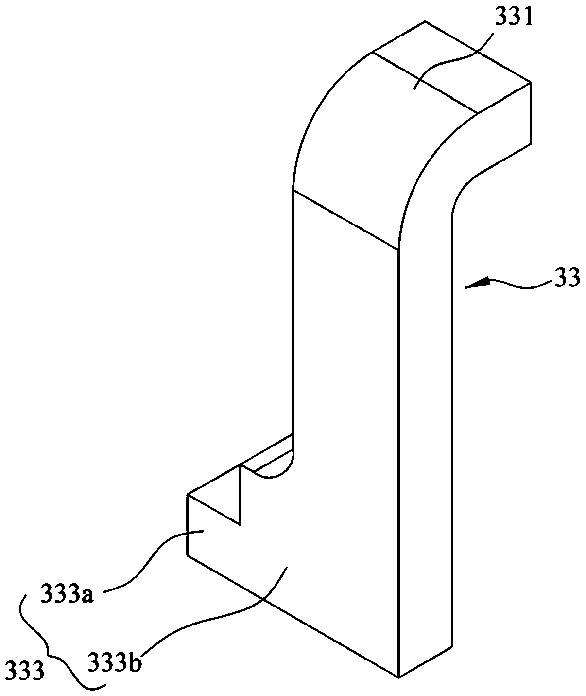
[0055] refer to figure 2 , the three-dimensional exploded view of the first preferred embodiment of the thinned inductance element embedded structure of the present invention, refer to Figure 5 , the side cross-sectional view of the first preferred embodiment of the thinned inductance element embedded structure of the present invention. like figure 2 As shown, the thinned inductance element embedding structure 100 of the present invention at least includes a base 3, a coil 5 and an electronic component 7, wherein a cavity 31 is formed on one side of the base 3, and the cavity 31 and There is an accommodating space, and the base 3 is preset with two terminals 33; wherein, the base 3 is made of insulating material, and the wall surrounding the cha...


PUM


Abstract

The invention provides a thin-type inductance element embedding structure at least including a base, a coil, and an electronic component, wherein the base has a cavity which has an accommodation space and two terminals are preset on the base, the coil and the electronic component are fixed in the accommodation space of the cavity, and the coil and the electronic component are in electrical connection through the two terminals. An element connection structure capable of establishing a basic circuit with at least two components, instead of a single active component or a single passive component, in the base is provided, so that the configuration density of the electronic components on the electronic circuit can be improved, the planning of the electronic circuit in an electronic device is facilitated, and the structure is suitable for thin electronic devices with strong functions.

Description

technical field [0001] A component connection structure, especially a thin inductive component embedding structure in which at least two components constitute a basic circuit structure is built in the base, which is helpful for the planning of the electronic circuit in the electronic device and improves the electronic performance. The arrangement density of components on an electronic circuit. Background technique [0002] In response to the miniaturization of IC process technology and the trend of thinner, lighter and smaller electronic information products, electronic components mounted on printed circuit boards have gradually evolved from plug-in components to surface mount devices (SMD). [0003] see figure 1 , is a structural diagram of an existing SMD inductance element. The magnetic core 1 has an upper end 11, a middle section 14 and a lower end 12 and is I-shaped, and the two sides of the upper end 11 and the lower end 12 have grooves 111 and 111', 121 and 121', an...

Claims


Application Information

Patent Timeline
Patent Type & Authority Patents(China)
IPC IPC(8): H05K1/18H01F27/06
Inventor 范云光
Owner 鸿磬电子(东莞)有限公司
Why Eureka
Try Eureka