Method of producing p-GaN low-resistance Ohm contact

An ohmic contact and p-gan technology, applied in the field of p-type gallium nitride, can solve the problem of large resistance, reduce contact resistance and improve device performance

Inactive Publication Date: 2009-07-15
EPITOP PHOTOELECTRIC TECH
View PDF3 Cites 1 Cited by
  • Summary
  • Abstract
  • Description
  • Claims
  • Application Information

AI Technical Summary

Problems solved by technology

[0006] The purpose of the present invention is to provide a method for preparing a p-GaN low-resistance ohmic contact to solve the problem of high resistance of the existing p-GaN ohmic contact

Method used


Image

  • Method of producing p-GaN low-resistance Ohm contact
  • Method of producing p-GaN low-resistance Ohm contact
  • Method of producing p-GaN low-resistance Ohm contact

Examples


Embodiment Construction

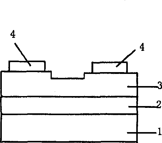
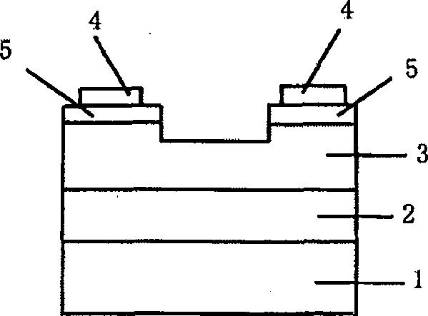
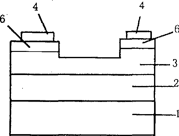
[0035] (1) Using Thomas Swan LP-MOCVD equipment for epitaxial wafer growth, the following three growth schemes are given for sample C.

[0036] 1) The first growth plan

[0037] (a) Load the (0001) orientation no-clean sapphire substrate into the reaction chamber, and 2 Heat to 1080°C and bake for 10 minutes under the atmosphere, and the pressure of the reaction chamber is 500Torr;

[0038] (b) Grow a GaN buffer layer with a thickness of 25nm at 550°C, the growth pressure is 500Torr, the flow rate of TMGa is 40mol / min, NH 3 The flow rate is 110mol / min;

[0039] (c) A 2μm GaN layer was grown at 1060°C, the growth pressure was 200Torr, the TMGa flow rate was 50μmol / min, NH 3 The flow rate is 110mol / min;

[0040] (d) A magnesium-doped GaN layer is grown on the GaN layer at a growth temperature of 800°C, a growth thickness of 500nm, a growth pressure of 200Torr, a TMGa flow rate of 50mol / min, and NH 3 The flow rate is 110mol / min; Cp 2 Mg is 140nmol / min;

[0041] (e) 5 cycle...


PUM

PropertyMeasurementUnit
thicknessaaaaaaaaaa
thicknessaaaaaaaaaa
thicknessaaaaaaaaaa

Abstract

A method for preparing a p-GaN low-resistance ohmic contact relates to a p-type gallium nitride (p-GaN). A method for preparing p-GaN low-resistance ohmic contacts is provided. Put the (0001)-oriented sapphire substrate into the reaction chamber, heat-treat the substrate under H2 atmosphere, lower the temperature and nitriding the substrate; grow the GaN buffer layer at lower temperature, and recrystallize the GaN buffer layer at higher temperature; epitaxially grow the GaN layer; Growth of Mg-doped GaN layer at lower temperature; growth of p-InGaN / p-AlGaN superlattice layer for 5 cycles at lower temperature; growth of p-InGaN cap layer on p-InGaN / p-AlGaN superlattice layer for 5 cycles . The results show that using p-InGaN / p-AlGaN superlattice as the top layer can obtain lower specific contact resistance.

Description

technical field [0001] The invention relates to a p-type gallium nitride (p-GaN), in particular to a preparation method of a p-GaN low-resistance ohmic contact using a p-AlGaN / p-InGaN superlattice as a top layer. Background technique [0002] In recent years, GaN-based wide-well-band semiconductor material has attracted much attention due to its wide application prospects in short-wavelength light-emitting devices, photodetection devices, and radiation-resistant, high-frequency and high-power devices, and has developed rapidly. These devices all involve P-type ohmic contacts, but good P-type ohmic contacts have always been one of the main factors restricting their further development. The low-resistance P-type ohmic contact of GaN-based materials is mainly restricted by the following two aspects: the lack of suitable contact metal materials, the work function of p-GaN materials is very large (7.5eV), and the metal Pt with the largest work function is only 5.65 eV; it is dif...

Claims


Application Information

Patent Timeline
Patent Type & Authority Patents(China)
IPC IPC(8): H01L21/04H01L21/20H01L21/205H01L33/00H01L31/18
CPCY02P70/50
Inventor 刘宝林张保平尹以安
Owner EPITOP PHOTOELECTRIC TECH
Why Eureka
Try Eureka