Method for manufacturing groove and its method for manufacturing image sensor

A technology of grooves and ditches, which is applied in the field of manufacturing metal oxide semiconductor image sensors, can solve problems such as difficult to control contours, achieve good contours, avoid bombardment damage, and be easy to control

Active Publication Date: 2009-07-22
SEMICON MFG INT (SHANGHAI) CORP +1
View PDF5 Cites 0 Cited by
  • Summary
  • Abstract
  • Description
  • Claims
  • Application Information

AI Technical Summary

Problems solved by technology

[0007] Therefore, the object of the present invention is to provide a method for forming a trench in a laminated dielectric layer and a method for its application in manufacturing a metal oxide semiconductor image sensor, so as to solve the problem of the existing metal oxide semiconductor image sensor for manufacturing copper interconnection lines. The problem that the profile is difficult to control when forming grooves in the sensor

Method used


Image

  • Method for manufacturing groove and its method for manufacturing image sensor
  • Method for manufacturing groove and its method for manufacturing image sensor
  • Method for manufacturing groove and its method for manufacturing image sensor

Examples


Embodiment Construction

[0028] In order to make the above objects, features and advantages of the present invention more comprehensible, specific implementations of the present invention will be described in detail below in conjunction with the accompanying drawings.

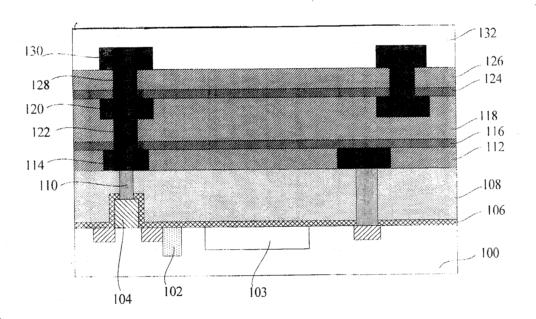
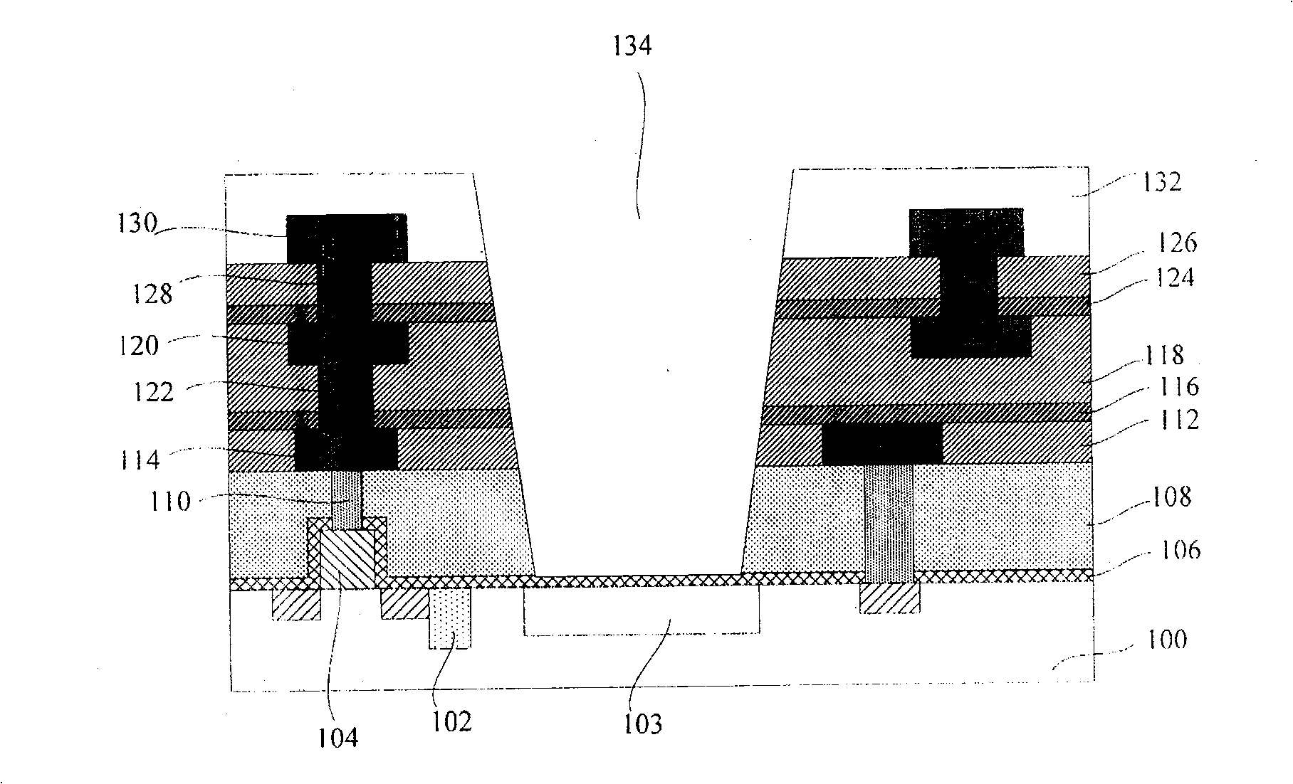
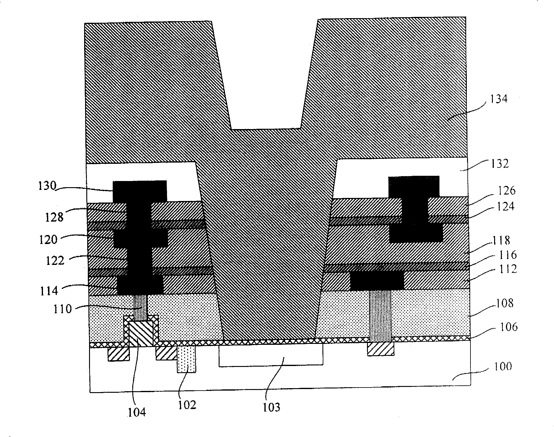
[0029] The method for forming trenches in stacked dielectric layers will be described in detail below in conjunction with embodiments. Figure 6 to Figure 11 It is a schematic cross-sectional view of the structure corresponding to each step of the embodiment of the method of the present invention.

[0030] Such as Figure 6 As shown, firstly, a semiconductor substrate 300 is provided, and the material of the semiconductor substrate 300 can be one of single crystal silicon, polycrystalline silicon, amorphous silicon, silicon-on-insulator, and a silicon-germanium composition. A first dielectric layer 310 is formed on the semiconductor substrate 300 . The first dielectric layer 310 is made of silicon oxide, silicon nitride, silicon carb...


PUM


Abstract

A method for forming a trench in a laminated dielectric layer, comprising: forming a first dielectric layer on a semiconductor substrate; forming a first opening in the first dielectric layer; filling the first opening in the first opening Sacrificial layer; at least a second dielectric layer is formed on the first dielectric layer, and a second opening is formed in the second dielectric layer, the second opening is located above the first opening, and the first The depth of the second opening is the same as the thickness of the second dielectric layer; filling the second opening with a second sacrificial layer; removing the first sacrificial layer and the second sacrificial layer. The method of the invention can form a better groove profile.

Description

technical field [0001] The invention relates to the technical field of semiconductor manufacturing, in particular to a method for forming a trench in a laminated dielectric layer and its application to manufacturing a metal oxide semiconductor image sensor. Background technique [0002] Metal oxide semiconductor image sensor (CMOS image sensor, CIS) is widely used in digital cameras, video cameras, handheld computers, camera phones and other devices due to its low power consumption, high response rate and other advantages. The main principle is: through The photosensitive unit receives the light signal and converts it into an electric signal through the photodiode, further processes the electric signal through the metal oxide semiconductor device, and transfers it to the storage medium. With the development of semiconductor manufacturing technology to higher technology nodes and the requirements for image sensor sensitivity and other performance, copper gradually replaces al...

Claims


Application Information

Patent Timeline
Patent Type & Authority Patents(China)
IPC IPC(8): H01L21/76H01L21/762H01L21/822H01L27/146
Inventor 卢普生杨建平
Owner SEMICON MFG INT (SHANGHAI) CORP
Why Eureka
Try Eureka