
Making method for memory capacitor

A technology for storage capacitors and manufacturing methods, applied in semiconductor/solid-state device manufacturing, circuits, electrical components, etc., to achieve the effect of improving effective doping concentration and conductivity

Active Publication Date: 2009-07-22
SEMICON MFG INT (SHANGHAI) CORP +1
View PDF5 Cites 0 Cited by
  • Summary
  • Abstract
  • Description
  • Claims
  • Application Information

AI Technical Summary

Problems solved by technology

[0006] Using HSG to replace flat polysilicon (Flat poly) as the semiconductor plate in MIS improves the capacity of the capacitor, but it is a big challenge for D / R

Method used


Image

  • Making method for memory capacitor
  • Making method for memory capacitor
  • Making method for memory capacitor

Examples


Embodiment Construction

[0064] The specific embodiments of the present invention will be described in detail below in conjunction with the accompanying drawings.

[0065] image 3 It is a flow chart of the first embodiment of the manufacturing method of the present invention.

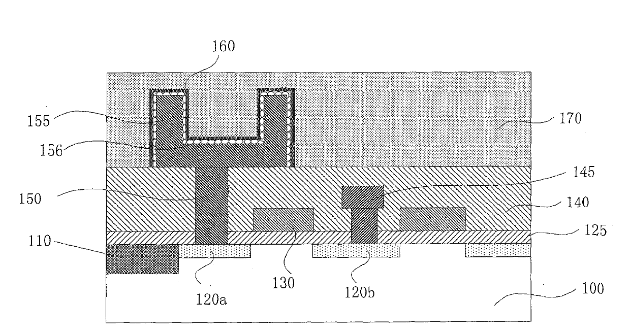
[0066] Such as image 3 As shown, a semiconductor substrate is provided on which a device layer, such as a metal oxide transistor (MOS), is formed. The metal oxide transistor includes a source, a drain and a gate, and a conductive channel is formed between the source and the drain. An insulating layer is deposited on the substrate on which the metal oxide transistor is formed, and a connection hole is formed by etching on the insulating layer ( S400 ).

[0067] Forming a capacitor first plate, such as doped polysilicon, on the insulating layer (S410). The first pole plate is electrically connected to the source of the MOS transistor on the substrate through the connection hole on the insulating layer. The thickness and sha...


PUM

PropertyMeasurementUnit
thicknessaaaaaaaaaa
thicknessaaaaaaaaaa

Abstract

A method for fabricating a storage capacitor includes that a semiconductor substrate provided with a device layer is deposited with an insulating layer and etched to form a connecting hole; a first polar plate is formed on the insulating layer; the rapid thermal annealing and oxidizing treatment is performed on the first polar plate; a dielectric layer is formed on the first polar plate; a second polar plate is formed on the dielectric layer. The method can increase the consistency when different polar voltages are sequentially exerted on the two sides of the capacitor, and prevent the damage on the capacitor polar plate caused by cleaning in the process of fabricating.

Description

technical field [0001] The invention relates to the technical field of semiconductor manufacturing, in particular to a method for manufacturing a storage capacitor. Background technique [0002] DRAM is a storage device widely used in electronics, communication and other fields. A dynamic memory storage unit generally includes a storage capacitor and a MOS transistor. The increase of its storage density needs to integrate more storage units per unit area and store more information per unit storage unit. Integrating more memory cells per unit area requires continuous reduction in device size, which depends on the development and progress of photolithography technology. Now 193nm exposure technology has begun to be used in production, and 157nm and immersion exposure technology has also been developed. Come out; the amount of information stored in a unit storage unit is determined by the capacity of the storage capacitor, and increasing the surface area of ​​the capacitor pl...

Claims


Application Information

Patent Timeline
Patent Type & Authority Patents(China)
IPC IPC(8): H01L21/822H01L21/8242H10B12/00
Inventor 虞肖鹏杨欣张复雄冯勇
Owner SEMICON MFG INT (SHANGHAI) CORP
Learn More