Method for producing a planar spacer, an associated bipolar transistor and an associated BiCMOS circuit arrangement

A bipolar transistor and spacer technology, applied in circuits, semiconductor/solid-state device manufacturing, electrical components, etc., to achieve cost-effective, improved electrical characteristics

Inactive Publication Date: 2009-08-05
INFINEON TECH AG
View PDF4 Cites 0 Cited by
  • Summary
  • Abstract
  • Description
  • Claims
  • Application Information

AI Technical Summary

Problems solved by technology

Since the result of this process is not self-adjusting, all fluctuations and tolerances of photolithography are included

Method used


Image

  • Method for producing a planar spacer, an associated bipolar transistor and an associated BiCMOS circuit arrangement
  • Method for producing a planar spacer, an associated bipolar transistor and an associated BiCMOS circuit arrangement
  • Method for producing a planar spacer, an associated bipolar transistor and an associated BiCMOS circuit arrangement

Examples


Embodiment Construction

[0023] The following diagrammatic description illustrates the concept of producing a planar spacer according to the present invention, especially when a planar spacer is used in bipolar transistors and related BiCMOS circuit devices.

[0024] In particular, the sacrificial mask is used as implant hardmask and foundation, so that planar spacers can be formed in a self-adjusting manner to connect multiple regions with one region as close as possible, which will be later Explain, for example, the intrinsic base of a single-multiple bipolar transistor.

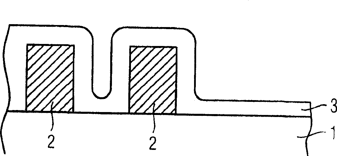
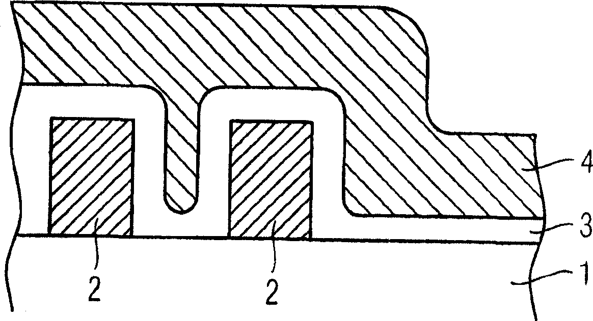
[0025] First, the method of producing a planar spacer according to the present invention, especially the method of producing a planar outer spacer, will be referred to Figure 1A-1F Be explained. Hereinafter, the term "planar outer spacer" means a substantially flat planar spacer formed on the sidewall of the mask pillar.

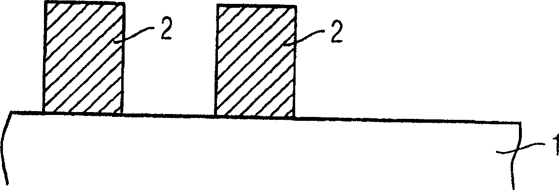
[0026] Such as Figure 1A As shown, first a sacrificial mask 2 is formed on the mounting substrate 1, for ...


PUM


Abstract

Method for producing a planar spacer, an associated bipolar transistor and an associated BiCMOS circuit arrangement. The invention relates to a method for production of a planar spacer, of an associated bipolar transistor and of an associated BiCMOS circuit arrangement, in which first and second spacer layers are formed after the formation of a sacrificial mask on a mount substrate. A first anisotropic etching process of the second spacer layer is carried out to produce auxiliary spacers. A second anisotropic etching step is then carried out, in order to produce the planar spacers, using the auxiliary spacers as an etch mask.

Description

technical field [0001] The present invention relates to a method of fabricating a planar spacer, to an associated bipolar transistor and to an associated BiCMOS circuit arrangement, and more particularly to a method of fabricating self-regulating single-multiple bipolar transistors with improved electrical characteristics in BiCMOS circuits. Background technique [0002] In bipolar transistors, in order to obtain a high cut-off frequency and reduce radio frequency noise, it must be kept in contact with and connected to the intrinsic base with the lowest possible resistance. This is particularly advantageous with a base connection as short as possible, preferably self-adjusting, and with low resistance. [0003] In the case of so-called "single-multiple bipolar transistors", this base connection region is usually defined photolithographically, that is to say not in a self-regulating manner. For example, photolithographically defined emitter pillar blocks are used as implante...

Claims


Application Information

Patent Timeline
Patent Type & Authority Patents(China)
IPC IPC(8): H01L21/8249H01L21/331
CPCH01L21/8249H01L29/66242
Inventor C·达尔A·蒂尔克
Owner INFINEON TECH AG
Why Eureka
Try Eureka