Method for manufacturing afebrile array wave-guide grating based on flat-plate wave-guide movement and delicate adjustment device

An arrayed waveguide grating and waveguide grating technology, which is applied to the coupling of optical waveguides and other directions, can solve the problems of highly difficult to accurately guarantee, spectral characteristics of insertion loss, complex process, etc., to improve wavelength adjustment accuracy, ensure constant focal length, spectral perfect effect

Active Publication Date: 2009-09-09
GUANGXUN SCI & TECH WUHAN
View PDF17 Cites 0 Cited by
  • Summary
  • Abstract
  • Description
  • Claims
  • Application Information

AI Technical Summary

Problems solved by technology

2) The adjustment of ITU-T wavelength is realized by temperature adjustment or plastic deformation, so the wavelength adjustment accuracy and repeatability are not very good; 3) The glue used for bonding is directly applied between the two contact surfaces, so some There is a height difference between part a and part b. In order to make up for this height difference, soft glue is coated between part a and the substrate. It is difficult to accurately ensure the height between part a and part b. At the same time, the waveguide size is only 5 or 6 microns , even a height difference on the order of micron will cause great deterioration of insertion loss and spectral characteristics; 4) if figure 2 As shown in the prior art, the two ends of the wavelength compensation rod are located on the upper surface of the AWG chip, but the two ends of the compensation rod are bonded by solder and solder. Melted at a high temperature of several hundred degrees, so the process is more complicated

Method used


Image

  • Method for manufacturing afebrile array wave-guide grating based on flat-plate wave-guide movement and delicate adjustment device
  • Method for manufacturing afebrile array wave-guide grating based on flat-plate wave-guide movement and delicate adjustment device
  • Method for manufacturing afebrile array wave-guide grating based on flat-plate wave-guide movement and delicate adjustment device

Examples


Embodiment Construction

[0051] The method for fabricating an athermal arrayed waveguide grating based on slab waveguide movement and the fine-tuning device of the present invention will be described in detail below in conjunction with the embodiments.

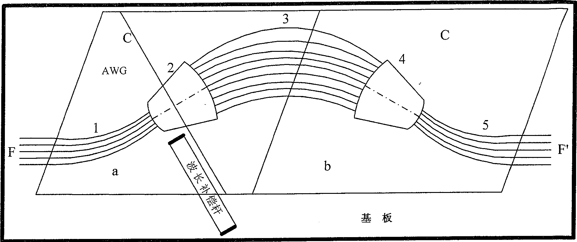
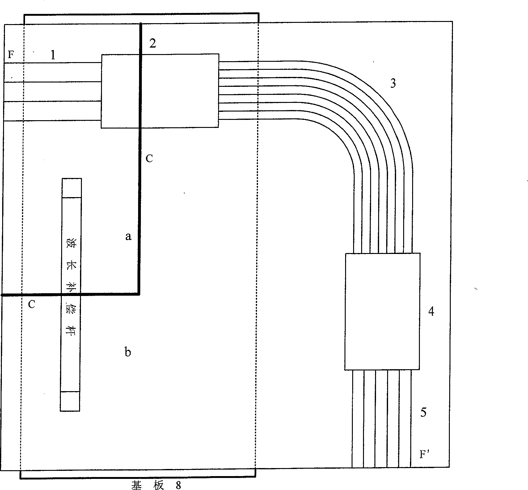
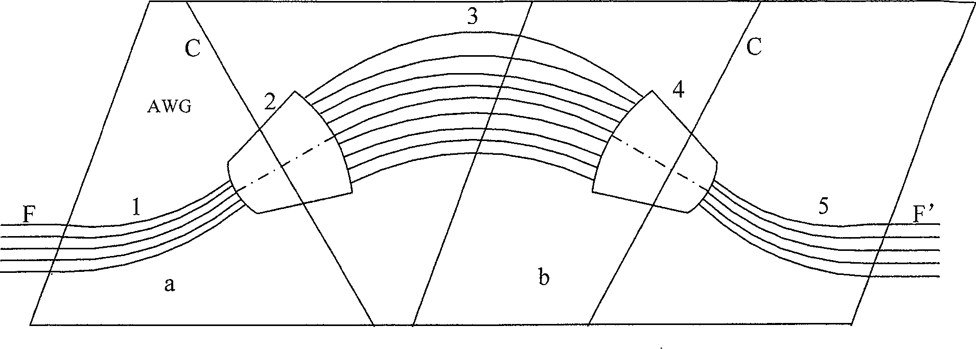
[0052] The present invention divides the chip into two parts a and b along the cutting line C on the input slab waveguide or the cutting line C on the output slab waveguide on the ordinary silicon-based silicon dioxide AWG chip produced by planar optical waveguide technology, and the part a includes the input waveguide 1 and a part of the input slab waveguide 2 , and part b includes the rest of the input slab waveguide 2 , the array waveguide 3 , the output slab waveguide 4 and the output waveguide 5 . The substrate 8 is placed under the two parts a and b of the AWG chip to play a role of fixing and supporting. The temperature compensation rod 6 is placed across the cutting line of the AWG chip. The surface is fixed, and one side of the glass baffle a...


PUM


Abstract

A method for fabricating an athermal arrayed waveguide grating based on slab waveguide movement and a fine-tuning device. The method: make the AWG chip and the input fiber array and the output fiber array reliably coupled and aligned; cut the AWG chip into a movable part and a fixed part along the cutting line; then glue the fixed part on the substrate; Put it on the substrate so that the cutting surfaces of the two parts are tightly coupled; along the connecting line of the two parts of the AWG chip, the side of the temperature compensation rod and the movable part are fixedly bonded together; use the fine adjustment device to adjust the temperature compensation rod Adjust the position of the athermal arrayed waveguide grating so that the output wavelength of the athermal arrayed waveguide grating meets the ITU-T regulations, and after the output spectrum of the athermal arrayed waveguide grating is the same as that of the AWG chip, fix and bond the other side of the temperature compensation rod to the fixed part . The fine-tuning device is a structure for fixing the substrate bonded with the AWG chip and adjusting the position of the temperature compensation rod on the substrate. The invention is simple and easy to implement, and greatly simplifies the process of making the athermal array waveguide grating.

Description

technical field [0001] The invention relates to a method for manufacturing an athermal arrayed waveguide grating. In particular, it involves the use of the thermal expansion and contraction of the temperature compensation rod to drive the relative movement of the a and b parts of the AWG chip, thereby compensating the wavelength drift caused by the temperature to make an athermal arrayed waveguide grating based on slab waveguide movement. Thermal arrayed waveguide grating method and fine tuning device. Background technique [0002] Stimulated by the huge bandwidth demand caused by the jet growth of data traffic represented by IP and the continuous emergence of new services, in the process of fully tapping the potential of optical communication technology and sparing no effort to use the huge bandwidth endowed by optical fiber Multiplexing (WDM) technology has gradually emerged with unique advantages such as easy expansion and low cost. The multiplexer and demultiplexer are...

Claims


Application Information

Patent Timeline
Patent Type & Authority Patents(China)
IPC IPC(8): G02B6/34
Inventor 周天红马卫东刘文赵秀丽祝业盛吴凡陈琳
Owner GUANGXUN SCI & TECH WUHAN
Why Eureka
Try Eureka