Grid dielectric layer manufacturing method

A manufacturing method and technology of gate dielectric layer, applied in semiconductor/solid-state device manufacturing, circuits, electrical components, etc., can solve problems such as low silicon-hydrogen bond energy, reduce threshold voltage, improve mobility, and improve reliability degree of effect

Inactive Publication Date: 2009-10-07
UNITED MICROELECTRONICS CORP
View PDF3 Cites 0 Cited by
  • Summary
  • Abstract
  • Description
  • Claims
  • Application Information

AI Technical Summary

Problems solved by technology

However, the bond energy of silicon-hydrogen bonds is low, so the number of silicon-hydrogen bonds will decrease after a period of operation in a high-temperature environment or semiconductor components, and then the number of captured carriers will increase again

Method used


Image

  • Grid dielectric layer manufacturing method
  • Grid dielectric layer manufacturing method
  • Grid dielectric layer manufacturing method

Examples


Embodiment Construction

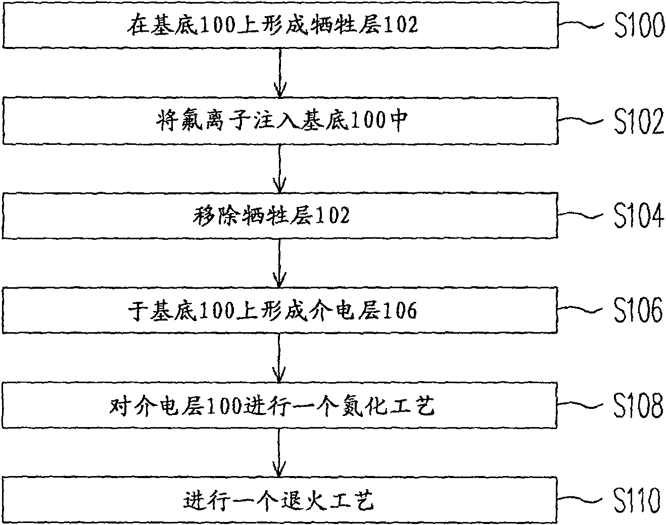
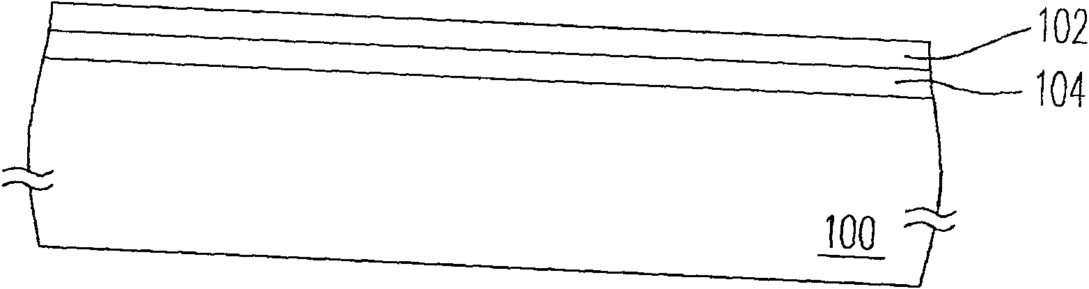
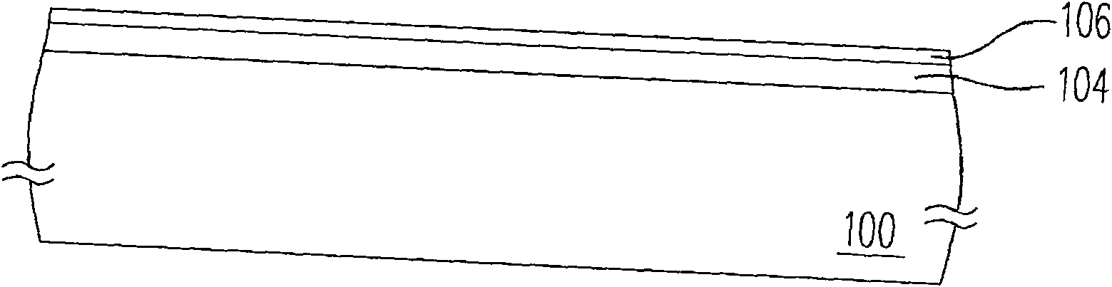
[0043] figure 1 What is shown is a flowchart of a method for manufacturing a gate dielectric layer according to an embodiment of the present invention. Figure 2A to Figure 2B Shown is a cross-sectional view of the manufacturing process of the gate dielectric layer according to an embodiment of the present invention.

[0044] First, please also refer to figure 1 and Figure 2A , proceed to step S100 to form a sacrificial layer 102 on the substrate 100 . The material of the sacrificial layer 102 is, for example, silicon oxide. The method of forming the sacrificial layer 102 is, for example, a thermal oxidation method.

[0045] Next, step S102 is performed to implant fluorine ions into the substrate 100 to form a doped region 104 . A method of implanting fluorine ions into the substrate 100 is, for example, an ion implantation method. Since the substrate 100 is covered with the sacrificial layer 102, the sacrificial layer 102 can prevent the fluorine ions from directly bom...


PUM


Abstract

A manufacture method for a grid dielectric layer includes the following steps of: firstly forming a sacrificial layer on a floor; then, injecting fluorinion into the floor; removing the sacrificial layer and then forming the dielectric layer on the floor.

Description

technical field [0001] The invention relates to a method for manufacturing a semiconductor element, in particular to a method for manufacturing a gate dielectric layer. Background technique [0002] With the decreasing trend of the size of metal oxide semiconductor (MOS) devices, there are more and more requirements on the quality of the gate dielectric layer, including the requirements on the interface characteristics between the gate dielectric layer and the substrate. [0003] However, there are many silicon bond breaks on the silicon substrate, and these bond break defects will make the interface between the gate dielectric layer and the substrate unstable, thereby increasing the threshold voltage (Threshold Voltage), and reducing the reliability of the semiconductor device. Shorten the lifetime of semiconductor components. [0004] In addition, since the broken bond exists at the interface between the gate dielectric layer and the substrate, when the current flows betw...

Claims


Application Information

Patent Timeline
Patent Type & Authority Patents(China)
IPC IPC(8): H01L21/28H01L21/31H01L21/336
Inventor 王俞仁颜英伟林建良詹书俨
Owner UNITED MICROELECTRONICS CORP
Why Eureka
Try Eureka