Printed circuit board including embedded capacitor and method of fabricating same

A technology for printed circuit boards and capacitors, which is used in the field of manufacturing PCBs and can solve problems such as poor electrical performance of electronic products

Inactive Publication Date: 2009-10-14
SAMSUNG ELECTRO MECHANICS CO LTD
View PDF5 Cites 0 Cited by
  • Summary
  • Abstract
  • Description
  • Claims
  • Application Information

AI Technical Summary

Problems solved by technology

[0026] In a high-frequency environment, the protrusion of the lower electrode layer 12a acts as a conductor, causing parasitic inductance, resulting in poor electrical performance of electronic products

Method used


Image

  • Printed circuit board including embedded capacitor and method of fabricating same
  • Printed circuit board including embedded capacitor and method of fabricating same
  • Printed circuit board including embedded capacitor and method of fabricating same

Examples


Embodiment Construction

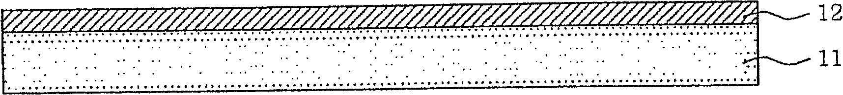
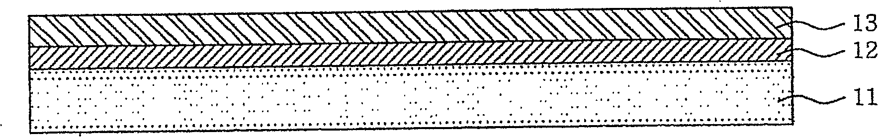
[0040] Hereinafter, a PCB including embedded capacitors and a manufacturing method thereof according to the present invention will be described in detail with reference to the accompanying drawings. In the drawings of the present invention, only one side of the PCB is processed, but actually both sides of the PCB are processed.

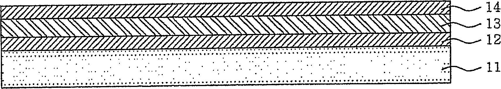
[0041] image 3 is a cross-sectional view of a PCB including embedded capacitors according to a first embodiment of the present invention.

[0042] Such as image 3 As shown, the PCB 100 includes an embedded capacitor according to the present invention, including an insulating layer 111, a lower electrode layer 112a and a circuit pattern 112b formed on the insulating layer 111, a dielectric layer 113a formed on the lower electrode layer 112a, and a dielectric layer 113a formed on the dielectric layer 113a. An insulating resin 115 is packaged between the upper electrode layer 114a and the lower electrode layer 112a and the circuit pattern 112b.

[004...


PUM


Abstract

Disclosed is a PCB including an embedded capacitor and a manufacturing method thereof, wherein a dielectric layer and an upper electrode layer are formed after the lower electrode layer of the embedded capacitor is formed, thereby providing a microcircuit pattern on a circuit layer having a lower electrode layer formed thereon .

Description

technical field [0001] The present invention generally relates to a printed circuit board (PCB) including embedded capacitors and a method of manufacturing the same, and more particularly to a PCB including embedded capacitors and a method of manufacturing the PCB, wherein a dielectric layer and an upper electrode are formed after forming a lower electrode layer of the embedded capacitor layer, whereby a microcircuit pattern is provided on the circuit layer having the lower electrode layer formed thereon. Background technique [0002] Recently, electronic technology has been developed toward building resistors, capacitors, integrated circuits (ICs), etc. into substrates in order to meet the needs of miniaturization and sophisticated functions of electronic products according to the development of the electronic industry. [0003] Typically, discrete chip resistors or discrete chip capacitors are usually mounted on most PCBs, but recently, PCBs in which resistors or capacitor...

Claims


Application Information

Patent Timeline
Patent Type & Authority Patents(China)
IPC IPC(8): H05K1/18H05K1/02H05K3/06H05K3/00
CPCH05K2203/0551H05K3/4644H05K3/184H05K3/108H05K3/0023H05K3/181H05K2201/09881H05K2201/09509H05K3/064H05K2201/0355H05K3/0082H05K1/162H05K1/16
Inventor 洪种国柳彰燮全皓植李硕揆
Owner SAMSUNG ELECTRO MECHANICS CO LTD
Why Eureka
Try Eureka