Fabricating method for semiconductor device

A manufacturing method and semiconductor technology, applied in semiconductor/solid-state device manufacturing, electrical components, circuits, etc., can solve problems affecting device performance, poor adhesion, etc., and achieve the effect of enhancing stability and enhancing adhesion

Active Publication Date: 2009-11-18
SEMICON MFG INT (SHANGHAI) CORP +1
View PDF3 Cites 0 Cited by
  • Summary
  • Abstract
  • Description
  • Claims
  • Application Information

AI Technical Summary

Problems solved by technology

However, in the process of removing the aluminum metal layer 20 not covered by the lead pad pattern 28a by etching, metal residues will be formed on the surface of the insulating layer 26, such as Figure 7 The residue 29 shown, the metal residue will cause the adhesion between the insulating layer 26 and other materials on it to deteriorate, thereby affecting the performance of the formed device

Method used


Image

  • Fabricating method for semiconductor device
  • Fabricating method for semiconductor device
  • Fabricating method for semiconductor device

Examples


Embodiment Construction

[0048] The specific embodiments of the present invention will be described in detail below in conjunction with the accompanying drawings.

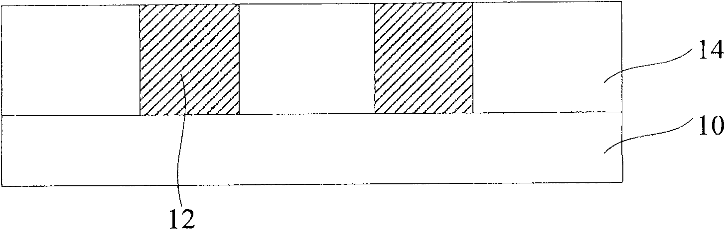
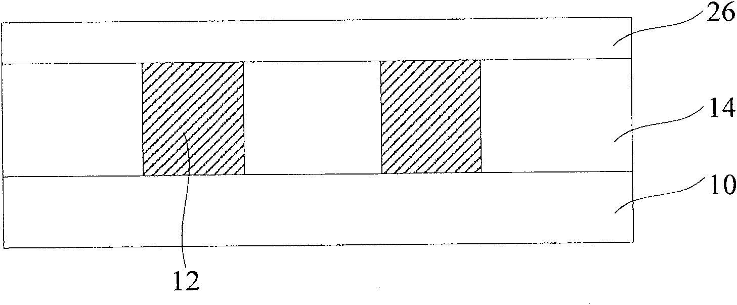
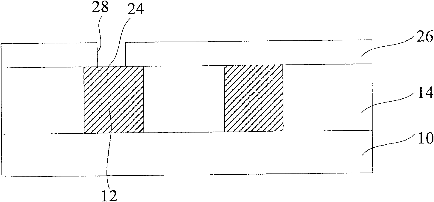
[0049] In the method of the present invention, before the photoresist layer is spin-coated on the aluminum metal layer, a barrier layer is first formed on the aluminum metal layer, then a photoresist layer is spin-coated on the barrier layer, and the patterned The photoresist layer forms a metal interconnection line pattern or a lead pad pattern; then etching removes the barrier layer and the aluminum metal layer not covered by the metal interconnection line pattern or the lead pad pattern to form a metal interconnection made of aluminum wire or lead pad. By forming a barrier layer between the photoresist layer and the aluminum metal layer, the photoresist layer can be prevented from diffusing into the grain gap of the aluminum metal layer, thereby reducing or eliminating metal residues caused thereby.

[0050] Figure 8 It is a flow cha...


PUM


Abstract

A manufacture method for a semiconductor apparatus includes the following steps of: providing a semiconductor structure; forming an aluminum metal layer on the semiconductor structure; forming an obstructing layer on the aluminum metal layer; forming a photosensitive resist layer on the obstructing layer; patterning the photosensitive resist layer to form a photosensitive resist pattern; removing the obstructing layer and the aluminum metal layer which are not covered by the photosensitive resist pattern; removing the photosensitive resist pattern. The method can reduce or eliminate the metal leftovers on the surface of an insulating layer (or passivation layer) on the lower surface of the aluminum metal layer after patterning the aluminum metal layer.

Description

technical field [0001] The invention relates to the technical field of semiconductor manufacturing, in particular to a manufacturing method of a semiconductor device. Background technique [0002] In the semiconductor manufacturing process, aluminum metal is used as a metal interconnect material or an outer lead pad material due to its low resistivity, good adhesion characteristics with dielectric materials such as silicon dioxide, and easy etching. Aluminum metal interconnects or lead pads are formed by processes of depositing an aluminum metal layer, photolithography, and etching the aluminum metal layer. US Patent No. 5785236 discloses a method of manufacturing aluminum lead pads. Figure 1 to Figure 4 It is a schematic cross-sectional view of the structures corresponding to each step of the manufacturing method of the aluminum lead pad disclosed in the US patent. [0003] Such as figure 1 As shown, the integrated circuit structure 10 has an interlayer dielectric layer...

Claims


Application Information

Patent Timeline
Patent Type & Authority Patents(China)
IPC IPC(8): H01L21/768H01L21/60
Inventor 康芸杨瑞鹏聂佳相
Owner SEMICON MFG INT (SHANGHAI) CORP
Why Eureka
Try Eureka