Semi-conductor light source device

A light source device and semiconductor technology, which is applied in the direction of semiconductor devices, light sources, lighting devices, etc., can solve the problems that semiconductor chips cannot be concentrated, the number of semiconductor chip packages is limited, and it is difficult to meet the requirements of light concentration.

Inactive Publication Date: 2010-01-13
LEADER ELECTRONICS
View PDF6 Cites 0 Cited by
  • Summary
  • Abstract
  • Description
  • Claims
  • Application Information

AI Technical Summary

Problems solved by technology

Although this kind of packaging structure can solve the heat dissipation problem of packaging multiple high-power chips, because only one side of the packaging structure can be attached to the semiconductor chip, the number of packages of the semiconductor chip is limited...

Method used


Image

  • Semi-conductor light source device
  • Semi-conductor light source device
  • Semi-conductor light source device

Examples


Embodiment Construction

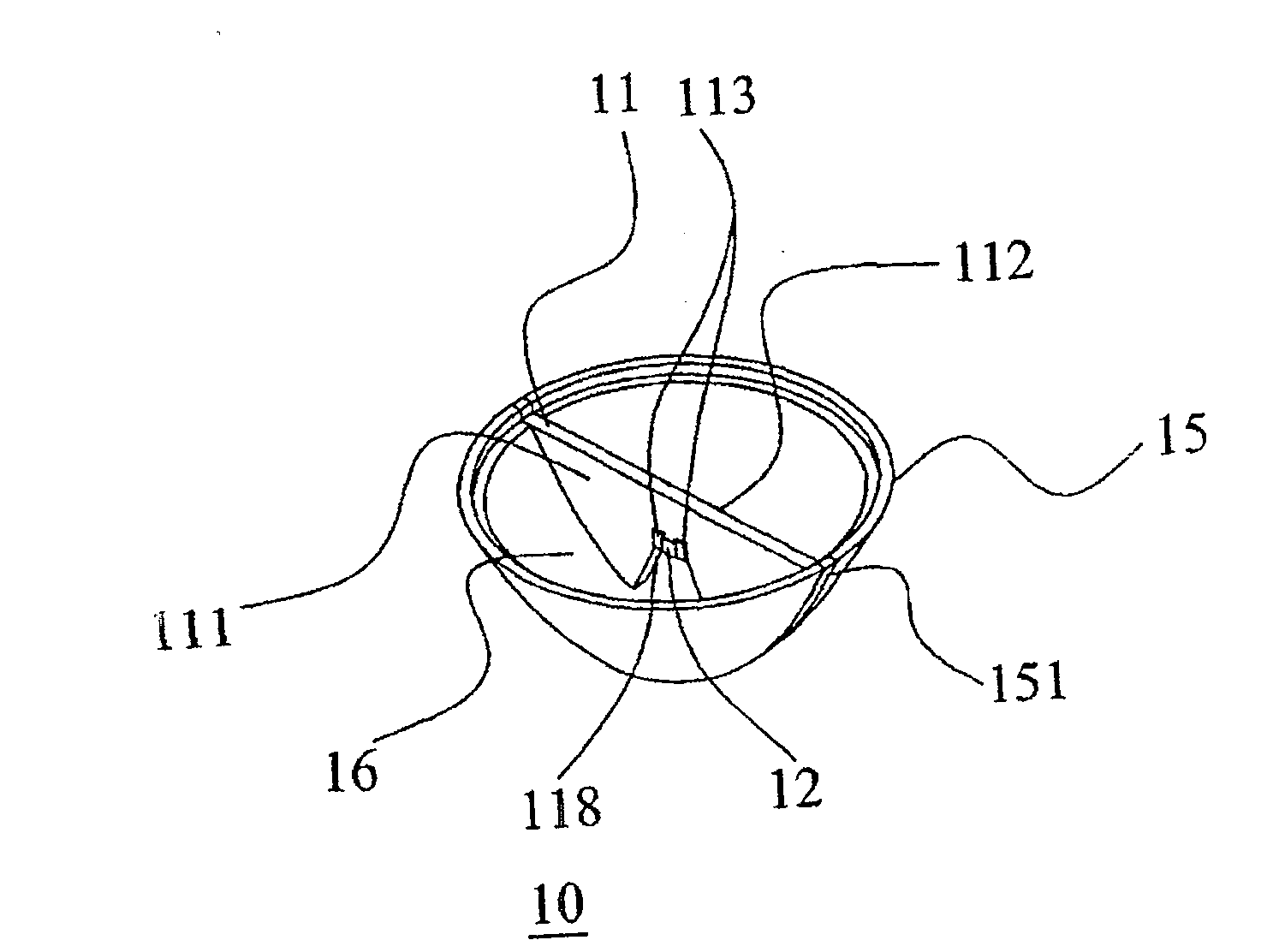
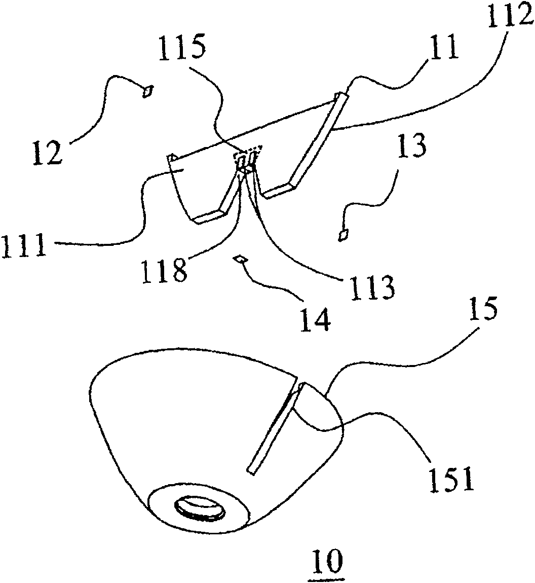
[0024] Figure 1-2 A semiconductor light source device 10 according to the first embodiment of the present invention is shown. The semiconductor light source device 10 includes a thermally conductive substrate 11 such as an aluminum substrate or a flat heat pipe, a semiconductor chip 12, 13, 14 such as a light emitting diode chip, and a poly Light cup 15.

[0025] Wherein, the condenser cup 15 has a light outlet 16, and the periphery of the light outlet 16 is provided with two grooves 151, so that the thermally conductive substrate 11 can be installed in the condenser cup 15 along the two grooves 151, and the condenser cup 15 The light generated by the semiconductor wafers 12, 13, and 14 is concentrated in the direction of the light outlet 16.

[0026] As shown in the figure, the thermally conductive substrate 11 has a first surface 111 and a second surface 112 for selectively attaching semiconductor chips 12, 13, 14 and other planes and side edges 118. The first surface 111, the s...


PUM


Abstract

A semiconductor light source device is provided. A semiconductor wafer is attached to and electrically connected to the side of a thermal conducting baseplate and then put into a concentration light cup. Light produced by the semiconductor wafer is concentrated into the direction of the light exit of the concentration light cup. Furthermore, a principal light source can be arranged in the concentration light cup at the same time. The principal light source is a plurality of semiconductor wafers which are evenly attached around an internal conductor and an external conductor that are arranged with the same axis and are isolated by an insulation layer. The semiconductor wafers are combined by means of serial connection, parallel connection or serial and parallel connection, and then are connected with the internal conductor and the external conductor which are used as power supply electrodes. Then the semiconductor light source device both with light concentration and heat dissemination effects is formed.

Description

【Technical Field】 [0001] The present invention relates to a semiconductor light source device, in particular to a semiconductor light source device that uses the sides and planes of a thermally conductive substrate to attach a semiconductor chip to make it a semiconductor light source device that combines light concentration and heat dissipation. 【Background technique】 [0002] Conventionally, various bulbs such as incandescent lamps, halogen lamps or fluorescent lamps are mostly used as the light source of the light source device. Recently, semiconductor chips such as light emitting diodes (LEDs) have the advantages of small size, power saving and long life, etc., they are gradually replaced and become extremely popular light emitting sources. [0003] For the structure of the light source device, a multi-chip, high-power LED package has become an inevitable trend requirement. For example, US Patent No. 6,492,725 named "Concentrically Leaded Power Semiconductor Device Package" pr...

Claims


Application Information

Patent Timeline
IPC IPC(8): H01L25/00H01L25/075H01L23/488H01L23/367F21K7/00F21K99/00
CPCH01L2924/0002
Inventor 陈国禔
Owner LEADER ELECTRONICS
Why Eureka
Try Eureka