Three-dimensional network for chemical mechanical polishing

A network structure, three-dimensional technology, applied in the field of polishing pads, can solve the problem of not developing materials

Active Publication Date: 2010-01-27
ROHM & HAAS ELECTRONICS MATERIALS CMP HLDG INC
View PDF9 Cites 0 Cited by
  • Summary
  • Abstract
  • Description
  • Claims
  • Application Information

AI Technical Summary

Problems solved by technology

Although composite materials are an improvement over monolayer structures, materials that simultaneously achieve ideal planarization efficiency and zero-defect formation have not yet been developed

Method used


Image

  • Three-dimensional network for chemical mechanical polishing
  • Three-dimensional network for chemical mechanical polishing
  • Three-dimensional network for chemical mechanical polishing

Examples


Embodiment Construction

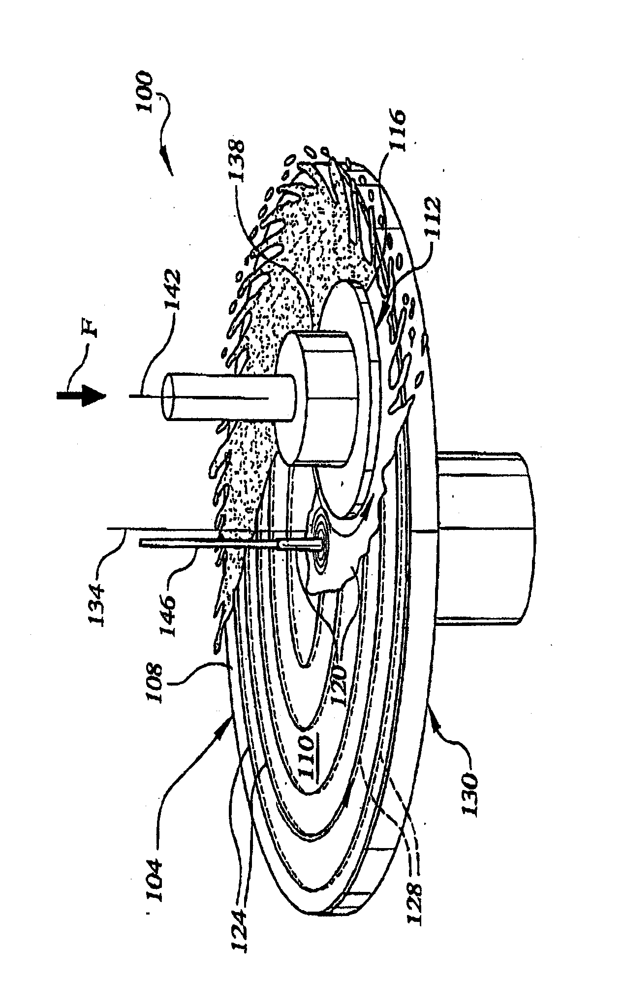
[0022] See attached picture, figure 1 The main features of a dual-axis chemical mechanical polisher (CMP) machine 100 suitable for use with the polishing pad 104 of the present invention are generally described. The polishing pad 104 generally includes a polishing layer 108 having a polishing surface 110 facing an article such as a semiconductor wafer 112 (processed or unprocessed) or other workpiece such as glass, a flat panel display or a magnetic information recording disc, etc., The polishing surface 116 of the workpiece is polished in the presence of the polishing medium 120 . Polishing media 120 moves through optional helical groove 124 having depth 128 . For simplicity, the term "wafer" is used in the general sense below. Furthermore, in this specification (including the claims), the term "polishing medium" includes particle-containing polishing solutions as well as particle-free solutions, such as abrasive-free and reactive liquid polishing solutions.

[0023] The p...


PUM


Abstract

Under the condition of existence color buffing medium (120), Polishing pad (104) used in at least one of color buffing magnetic, photics and semi-conductor substrate web. Polishing pad (104) includes three-dimensional network structure of interconnect unit (225). interconnect unit (225) is netted, convenient for fluid flow and remove the color buffing debris. Many color buffing element (208, 308, 408) come into being interconnect unit (255) three-dimensional network structure. Color buffing element (208, 308, 408) is provided with first tag end of first neighbouring element which connect to the first juncture (209, 309, 409), and the second tag end of second neighbouring element which connect to the second juncture (209, 309, 409), the cross sectional area is 30% between the first and second juncture (209, 309, 409). multitime colo(u)r buffing operational work is keep in line with glazed surface (200, 300, 400) which is composed of many color buffing element (208, 308, 408).

Description

technical field [0001] The present invention relates generally to the field of polishing pads for chemical mechanical polishing. In particular, the present invention relates to chemical mechanical polishing pads having polishing structures for chemical mechanical polishing of magnetic, optical, and semiconductor substrates. Background technique [0002] During the fabrication of integrated circuits and other electronic devices, layers of conductive, semiconducting, and dielectric materials are deposited onto and removed from the surface of semiconductor wafers. Thin layers of conducting, semiconducting and dielectric materials can be deposited using a number of deposition techniques. Conventional deposition techniques in modern wafer processing include physical vapor deposition (PVD) (also known as sputtering), chemical vapor deposition (CVD), plasma enhanced chemical vapor deposition (PECVD), and electrochemical plating, among others. Common removal techniques include wet...

Claims


Application Information

Patent Timeline
Patent Type & Authority Patents(China)
IPC IPC(8): B24D17/00B24B29/00H01L21/304B24D99/00
Inventor G·P·马尔多尼
Owner ROHM & HAAS ELECTRONICS MATERIALS CMP HLDG INC
Why Eureka
Try Eureka