Method for forming capacitor and random access memory unit

A random access memory and capacitor technology, applied in the manufacture of electrical components, circuits, semiconductor/solid-state devices, etc., can solve the problems of reducing the surface area of ​​capacitors, reducing capacitance, etc., to improve capacitance, increase surface area, and uniform atomic size. consistent effect

Inactive Publication Date: 2010-02-17
SEMICON MFG INT (SHANGHAI) CORP +1
View PDF5 Cites 0 Cited by
  • Summary
  • Abstract
  • Description
  • Claims
  • Application Information

AI Technical Summary

Problems solved by technology

[0010] like Image 6 As shown, when the polysilicon layer formed with hemispherical particles in the prior art is observed with an electronic scanning display mirror, due to the poor control of the size and density of the hemispherical particles, as the size of the semiconductor device decreases, it is easy to cause the gap between the hemispherical particles. A connection is created, the surface area of ​​the capacitor is reduced, and the capacitance is reduced

Method used


Image

  • Method for forming capacitor and random access memory unit
  • Method for forming capacitor and random access memory unit
  • Method for forming capacitor and random access memory unit

Examples


Embodiment

[0039] This embodiment provides a method for forming a capacitor, refer to the attached Figure 7 The process flow chart shown includes the following steps: execute step S301, forming uniform discrete atomic islands on a semiconductor substrate with an interlayer dielectric layer and a polysilicon layer in sequence; execute step S302, perform an annealing process, and make the atoms The island reacts with the polysilicon layer to form discrete spherical particles; perform step S303, use the discrete spherical particles as a mask, etch the polysilicon layer and the interlayer dielectric layer, and form grooves in the interlayer dielectric layer; perform step S304, A first conductive layer, an insulating dielectric layer and a second conductive layer are sequentially formed on the interlayer dielectric layer inside and outside the groove.

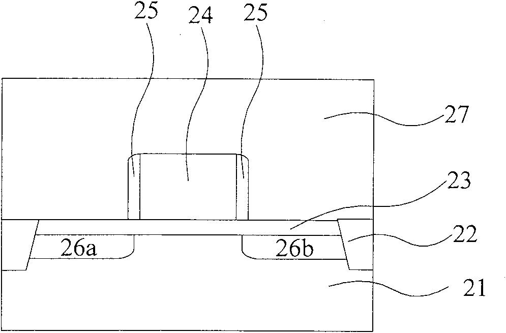
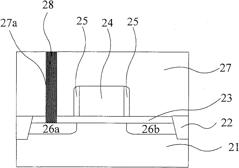
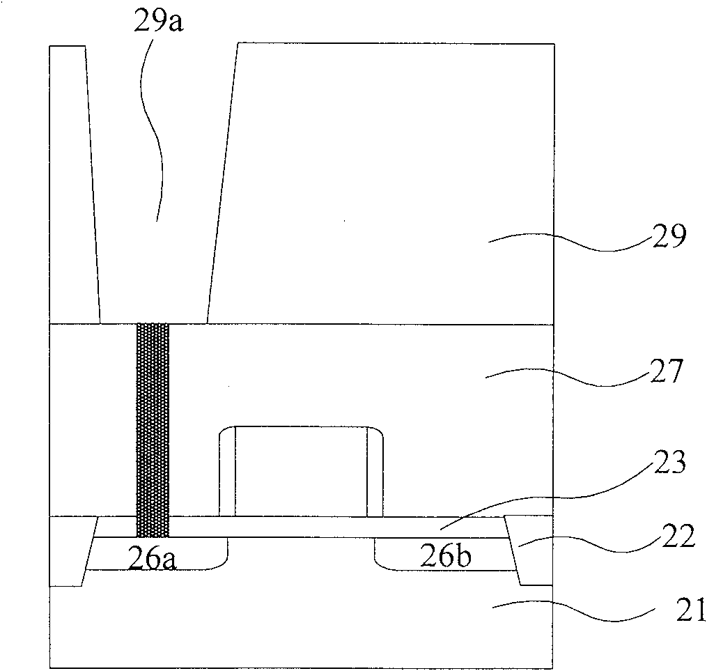
[0040] Figure 8 to Figure 12 It is a structural schematic diagram of an embodiment of forming a capacitor in the present invention. like ...


PUM

PropertyMeasurementUnit
depthaaaaaaaaaa
diameteraaaaaaaaaa
distanceaaaaaaaaaa

Abstract

Disclosed is a capacitor formation method, including the following steps: developing even discrete atom islands on a semiconductor substrate which has a dielectric interlayer and a polycrystalline silicon layer in sequence; processing annealing so as to enable the atom islands to react with the polycrystalline silicon layer to form discrete spherical grains; with the discrete spherical grains as amask, etching the polycrystalline silicon layer and the dielectric interlayer and developing a groove in the dielectric interlayer; and developing a first conduction layer, an insulating medium layerand a second conduction layer sequentially on the dielectric layer inside and outside the groove. The invention further provides a method for forming a random access memory cell. Since the atoms arecontrollable in size and density and the conductive grains formed after annealing are also controllable in size and density, the conductive grains will not be connected along with the minimizing of the size of the semiconductor, thus increasing the surface of the capacitor and improving capacitance.

Description

technical field [0001] The invention relates to the technical field of semiconductors, in particular to a method for forming a capacitor and a random memory unit. Background technique [0002] Random access memory is a widely used integrated circuit device. Currently common RAM units are mostly composed of transistors and capacitors. Capacitors are used to store charges to provide electronic information, and should have a large enough capacitance to avoid data loss and reduce the frequency of charging updates. [0003] With the increasing integration of semiconductor devices in the manufacturing process of integrated circuits, the density of random access memory storage units is also increasing, and the area that capacitors can use in random access memory storage units is smaller. In order to maintain reliable performance while reducing the area of ​​the capacitors, it is important to maintain the capacitance of each capacitor while reducing the area occupied by the capaci...

Claims


Application Information

Patent Timeline
Patent Type & Authority Patents(China)
IPC IPC(8): H01L21/822H01L21/8242
Inventor 季华季明华三重野文健
Owner SEMICON MFG INT (SHANGHAI) CORP
Why Eureka
Try Eureka