
Optical device package and optical semiconductor device using the same

A technology of optical components and components, applied in the direction of semiconductor devices, semiconductor/solid-state device parts, semiconductor lasers, etc., can solve the problems of reduced thermal conductivity of molded resin, increased high-frequency transmission loss, and reduced optical characteristics, etc., to reduce optical Reduced characteristics, good high-frequency characteristics, and good heat dissipation

Active Publication Date: 2010-02-24
MITSUBISHI ELECTRIC CORP
View PDF7 Cites 0 Cited by
  • Summary
  • Abstract
  • Description
  • Claims
  • Application Information

AI Technical Summary

Problems solved by technology

However, the thermal conductivity of molded resin is significantly lower than that of metal wire rings, and in the high-power LDs that have become popular in recent years, there are problems in optical characteristics due to poor heat dissipation and light spot shift due to deformation at high temperatures. falling situation
[0016] In the case of the third known example, since the lead support portion supporting the lead pin and the ground pin by molded resin is provided, the lead pin and the ground pin protrude only from the front end portion thereof, and the lead tube is opposed to the lead tube at the lead support portion. Most of the entire length of the pins and ground pins are resin-sealed. For this reason, the distance between the LD chip and the ground layer on the surface of the resin substrate increases, which increases the inductance and high-frequency propagation loss, and further When the output characteristics of the laser are affected and it is difficult to achieve good high-frequency characteristics

Method used


Image

  • Optical device package and optical semiconductor device using the same
  • Optical device package and optical semiconductor device using the same
  • Optical device package and optical semiconductor device using the same

Examples


Embodiment approach 1

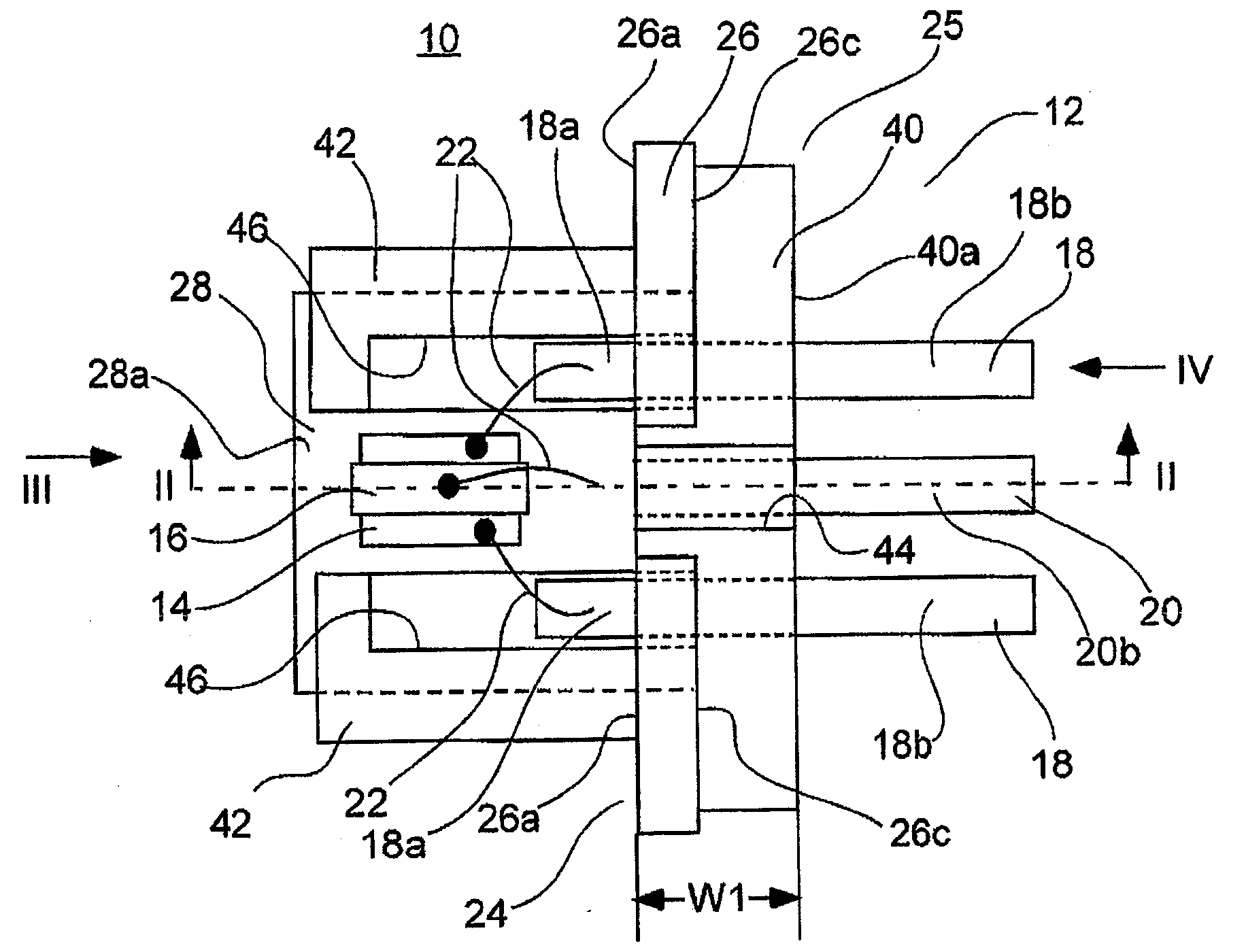
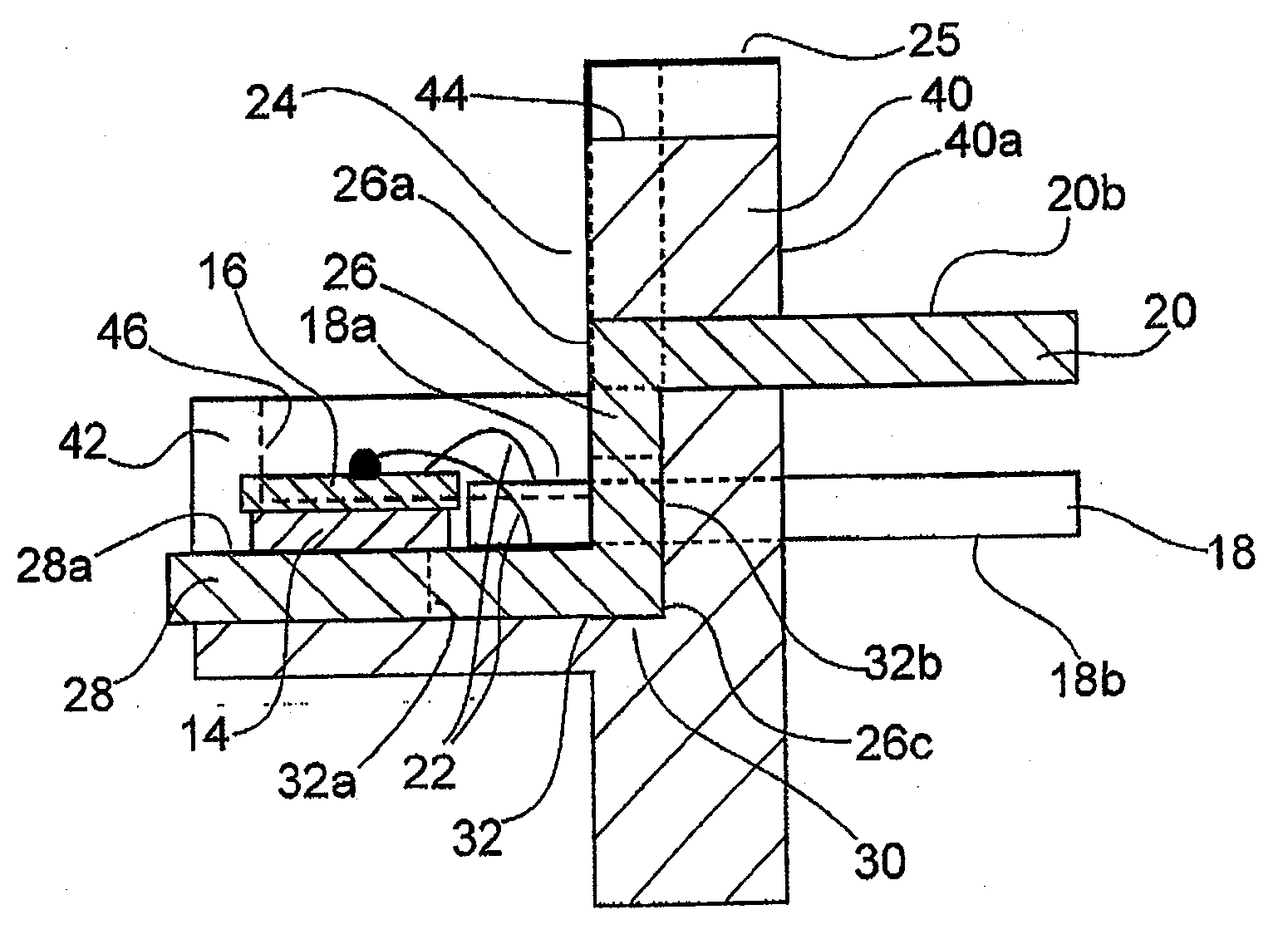
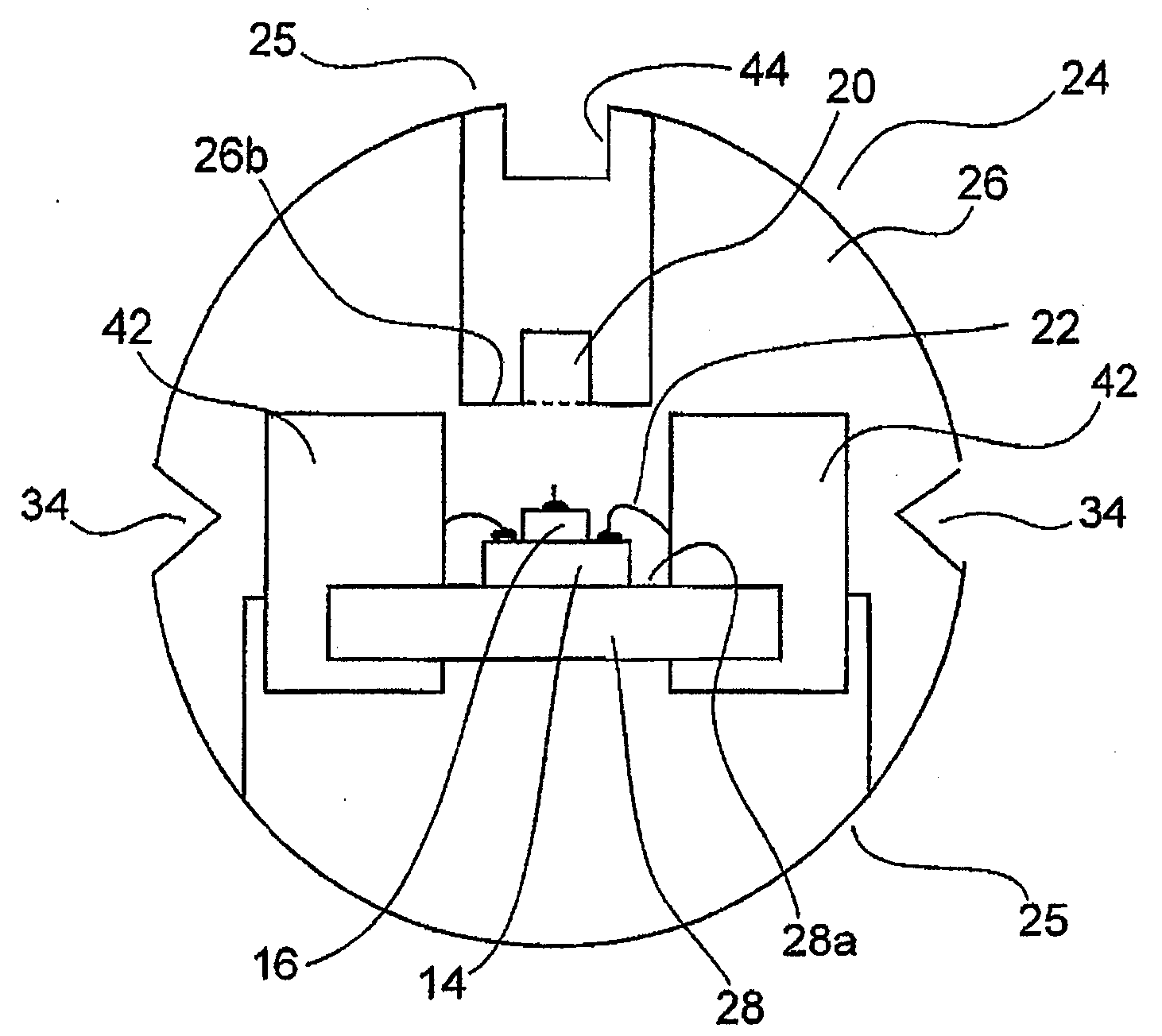
[0035] figure 1 is a plan view of an LD device according to one embodiment of the present invention. figure 2 yes figure 1 A cross-sectional view in the direction of the arrow in the II-II cross-section of the shown LD device. image 3 From figure 1 Front view of the LD device viewed in the arrow direction III. Figure 4 From figure 1 Bottom view of the LD device viewed in the arrow direction IV. Figure 5 It is a perspective view showing the positional relationship between the metal base and the lead electrodes of the LD device according to one embodiment of the present invention. Figure 6 is a perspective view of an LD device according to one embodiment of the present invention. In the drawings, the same symbols represent the same or corresponding components.

[0036] Such as figure 1As shown, the LD device 10 is composed of an LD assembly 12, an LD chip 16 installed in the LD assembly 12 by an auxiliary support (submount) 14, an electrode (not shown) connectin...


PUM


Abstract

The invention aims to constitute a package for an optical element, reduced in the deterioration of optical characteristics upon operation of an optical element and having excellent high-frequency characteristics while being inexpensive. The package for the optical element in reference to this invention is equipped with: a metal frame 24, having a substrate 26 constituted of a metal plate and a rectangular die pad unit 28, raised by bending the substrate 26 by 90 degrees; a signal lead pin 18 orthogonal to the principal surface of the substrate 26 and extended into the reverse direction of thedie pad unit 28 with respect to the substrate 26 while being arranged so as to be apart from the metal frame 24; and a resin mold unit 25, closely contacted with the principal surface of the substrate26 and provided with a plate type resin substrate 40 along the substrate 26 while the signal lead pin 18 is projected out of the surface of the resin substrate 40 so that the circumference of the signal lead pin 18 is buried and the metal frame 24 as well as the signal lead pin 18 are fixed thereto.

Description

technical field [0001] The present invention relates to a module for an optical element and a semiconductor device using the module, and more particularly to an optical device equipped with an optical element for receiving and transmitting high-frequency signals used in information electronic equipment or information communication equipment, etc. A component for an element, and an optical semiconductor device using the same. Background technique [0002] In recent years, the broadbandization of optical communication has been promoted, and with the spread of public communication networks using optical fibers, it has been increasingly required to transmit a large amount of information at low cost. Therefore, the amount of information handled by information electronic devices is also increasing day by day. Therefore, an inexpensive information electronic device that can process a large amount of information at high speed and has high reliability is required. [0003] Even amon...

Claims


Application Information

Patent Timeline
Patent Type & Authority Patents(China)
IPC IPC(8): H01S5/022H01L23/02
CPCH01L2224/48091H01L2224/45124H01L2224/48465H01L2224/45144H01L2924/30107H01L2924/3011
Inventor 藤野纯司田中秀幸森健三
Owner MITSUBISHI ELECTRIC CORP
Learn More