Eureka AIR delivers breakthrough ideas for toughest innovation challenges, trusted by R&D personnel around the world.

High speed processing method for realizing superfine crystal grain structure on metallic material surface

A metal material, ultra-fine grain technology, applied in the field of ultra-fine grain structure, can solve the problems of large consumption of trays and pellets, large surface roughness, complicated operation procedures, etc., and achieves strong applicability and high surface quality. , the effect of simple processing methods

Active Publication Date: 2010-03-24
INST OF METAL RESEARCH - CHINESE ACAD OF SCI
View PDF5 Cites 6 Cited by
  • Summary
  • Abstract
  • Description
  • Claims
  • Application Information

AI Technical Summary

Problems solved by technology

However, the surface roughness of the sample obtained by this processing technology is relatively large at present, which cannot meet the requirements of practical application, which limits its promotion in industry, and the shape of the processed sample also has great limitations.
In addition, the operating procedures are relatively cumbersome, and the consumption of trays and pellets used for grinding is large, resulting in increased costs

Method used


Image

  • High speed processing method for realizing superfine crystal grain structure on metallic material surface
  • High speed processing method for realizing superfine crystal grain structure on metallic material surface
  • High speed processing method for realizing superfine crystal grain structure on metallic material surface

Examples


Embodiment 1

[0026] Treatment of pure copper materials using surface high-speed deformation technology:

[0027] Equipment: Surface high-speed deformation processing equipment;

[0028] Spindle speed: 600rpm;

[0029] Deformation strain rate: 10 3 -10 4 the s -1 ;

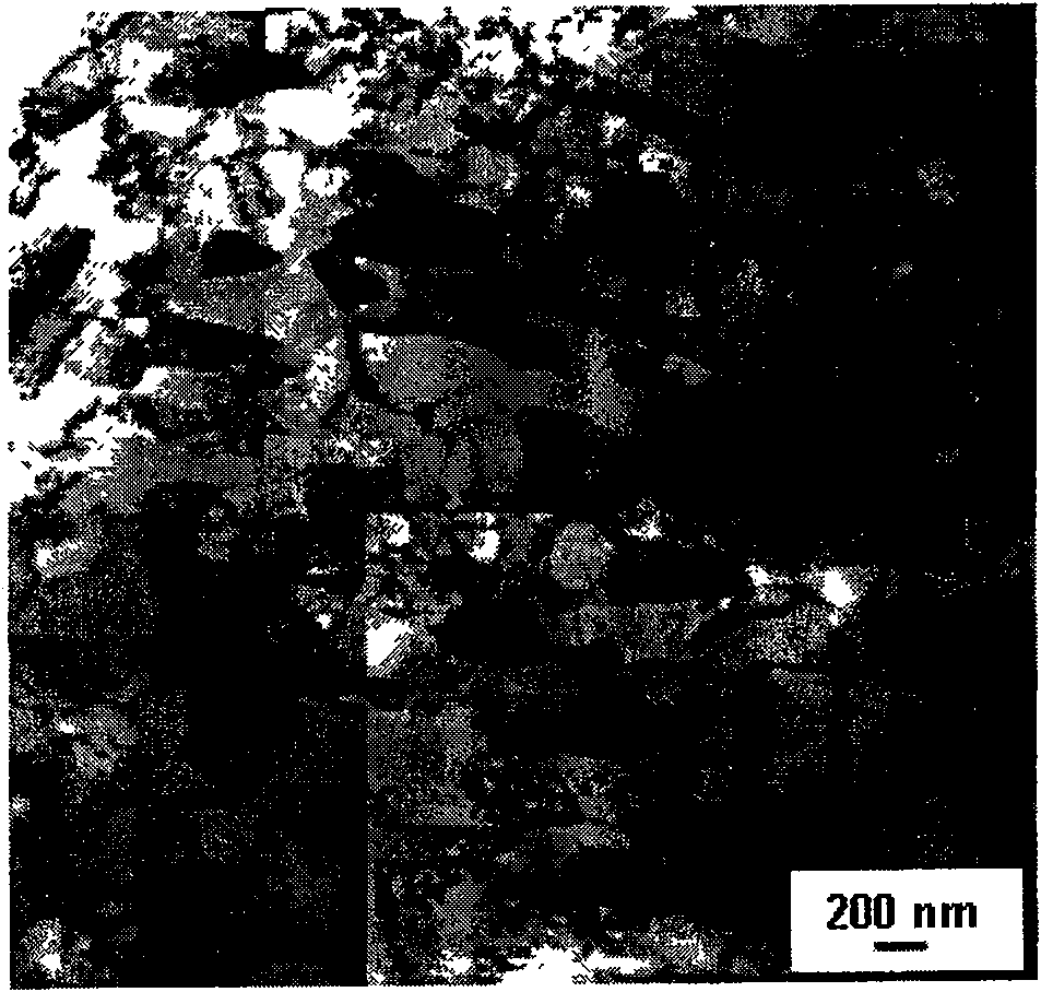
[0030] Deformation strain: 3-5;

[0031] Deformation temperature: 20°C;

[0032] Processing passes: 8;

[0033] Pure copper material: purity 99.97% (weight percent), annealed at 600° C. for 3 hours, grain size 20 μm.

[0034] Treatment to obtain pure copper materials with surface refinement, such as figure 1 , the thickness of the surface layer is about 60 μm, and its microstructure is mainly characterized by nearly equiaxed submicron grains / sub-grains, with a short axis dimension of 164nm and a long axis dimension of 351nm.

Embodiment 2

[0036] Treatment of pure copper materials using surface high-speed deformation technology:

[0037] Equipment: Surface high-speed deformation processing equipment;

[0038] Spindle speed: 1000rpm;

[0039] Deformation strain rate: 10 3 -10 4 the s -1 ;

[0040] Deformation strain: 3-5;

[0041] Deformation temperature: 20°C;

[0042] Processing passes: 8;

[0043] Pure copper material: purity 99.97%, annealed at 600°C for 3 hours, grain size 20μm.

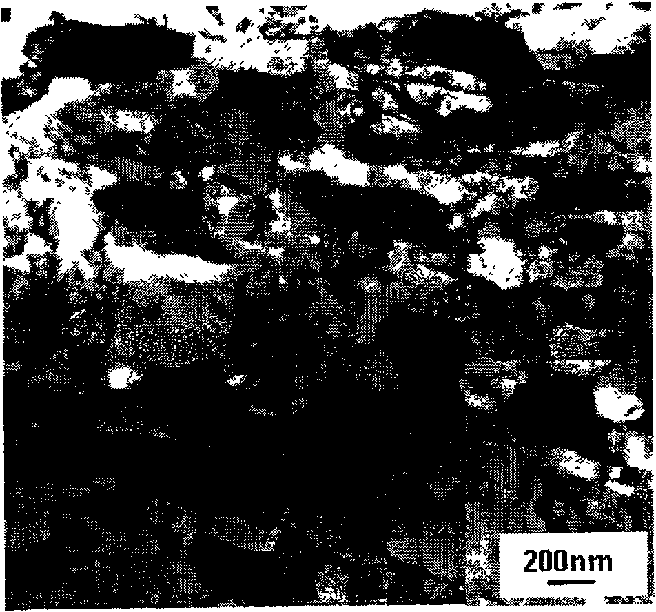
[0044] The processed surface structure is as figure 2 , the thickness of the surface layer is about 30 μm, the short axis dimension is 178nm, and the long axis dimension is 587nm.

Embodiment 3

[0046] Treatment of pure copper materials using surface high-speed deformation technology:

[0047] Equipment: Surface high-speed deformation processing equipment;

[0048] Spindle speed: 600rpm;

[0049] Deformation strain rate: 10 3 -10 4 the s -1 ;

[0050] Deformation strain: 3-5;

[0051] Deformation temperature: 20°C;

[0052] Processing passes: 6;

[0053] Pure copper material: purity 99.97%, annealed at 600°C for 3 hours, grain size 20μm.

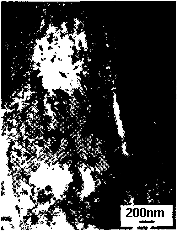
[0054] The thickness of the treated surface layer is about 30 μm, the short axis dimension is 158nm, and the long axis dimension is 604nm.


PUM

PropertyMeasurementUnit
deformation temperatureaaaaaaaaaa
thicknessaaaaaaaaaa

Abstract

The invention relates to a method for processing the high-speed deformation on the surface of metallic material with nano structure, and particularly provides a method for realizing high-speed processing of the organization structure of ultra-fine grains. On the condition of room temperature or low temperature, by adopting a mechanical treatment method with high-speed plastic deformation, the nanoscale bulky crystalline grain structure on the surface layer of the metallic material is refined as equiaxial submicron crystalline grain or nano crystalline grain to form an ultra-fine organization structure of the crystalline grain on the surface layer of the metallic material. With the increase of the depth to the processing surface, the size of microstructure has the change of gradient, increasing from nanoscale and submicron size to micron size. Compared with the existing processing method for forming a surface ultra-fine crystalline grain structure, the high-speed processing method of the invention greatly reduces the roughness of the surface of the processed metallic material and increases the thickness of a deformation layer, and has simple processing method and high working efficiency.

Description

technical field [0001] The invention relates to a treatment method for high-speed deformation of the surface of a metal material with a nanostructure, and in particular provides a high-speed processing method for realizing an ultra-fine grain structure on the surface of a metal material, forming nano-sized and sub-micron-sized ultra-fine particles on the surface of the metal material. Grain structure. Background technique [0002] Nanomaterials are single-phase or multi-phase crystalline materials composed of substructures with a structural size less than 100nm. Since the grain boundaries of nanomaterials occupy a large proportion, nanomaterials usually have excellent properties that are different from and often superior to ordinary polycrystalline materials. , such as high strength, high diffusion coefficient, good electrical and magnetic properties. [0003] At present, research in the field of nanostructured materials mainly focuses on the synthesis, preparation, structu...

Claims


Application Information

Patent Timeline
Patent Type & Authority Patents(China)
IPC IPC(8): C21D7/04C22F1/00
Inventor 李文利陶乃镕卢柯
Owner INST OF METAL RESEARCH - CHINESE ACAD OF SCI
Why Eureka
Eureka Blog
Learn More