A semiconductor pump micro-slice laser

A technology of microchip lasers and semiconductors, applied in the field of lasers, can solve problems affecting the structure, application and cost of semiconductor pumps, and achieve the effects of easy implementation and adjustment, cost saving, and prolonging life

Inactive Publication Date: 2007-08-01
SHANGHAI BRANCH FUZHOU GAOYI COMM CO LTD
View PDF0 Cites 5 Cited by
  • Summary
  • Abstract
  • Description
  • Claims
  • Application Information

AI Technical Summary

Problems solved by technology

The conventional frequency-doubling crystal KTP104 microchip is very small, and it is fixed by glue in the laser system, that is, it should be discarded after the pumped area is damaged, which seriously affects the application and cost of the semiconductor pump structure.

Method used


Image

  • A semiconductor pump micro-slice laser
  • A semiconductor pump micro-slice laser
  • A semiconductor pump micro-slice laser

Examples


Embodiment

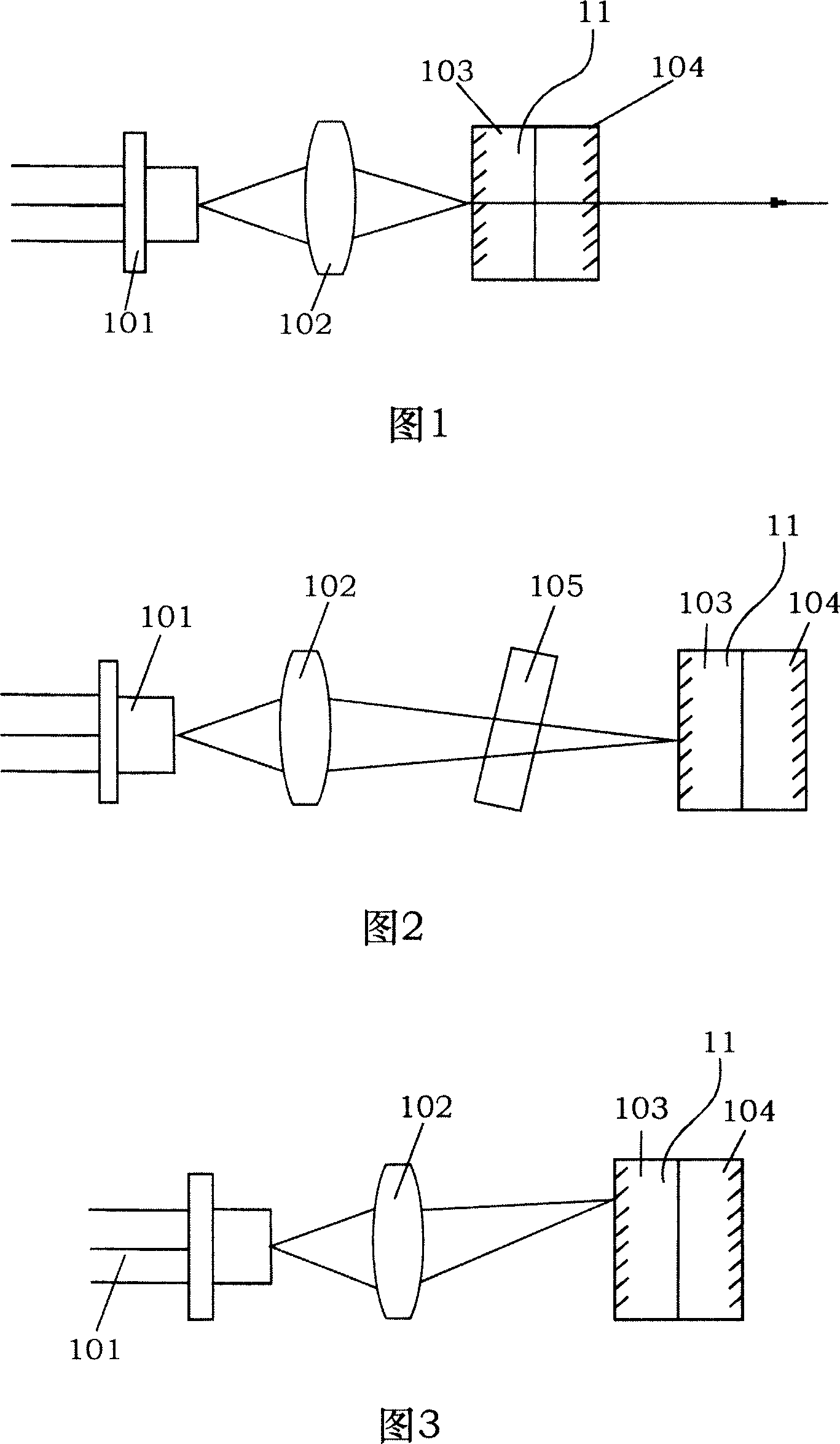
[0021] Embodiment 2: As shown in FIG. 3 , the optical lens coupling system 102 is made rotatable, and its central axis is offset parallel to the rotational central axis, so as to achieve the goal of moving the pumping point.

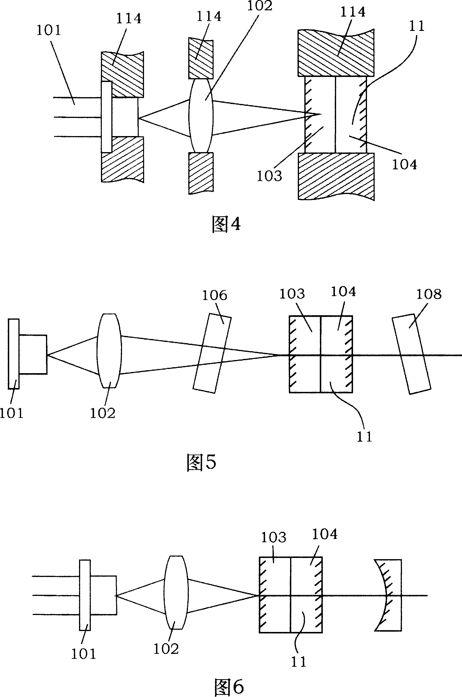
[0022] The third embodiment: as shown in Figure 4, a mechanical structure 114 is set outside one, two or three of the pumping source semiconductor laser 101, the optical lens coupling system 102 and the microchip laser 11, so that they pass through the light vertically The surface translation of the direction can make the position of the pumping spot on the microchip laser 11 move.

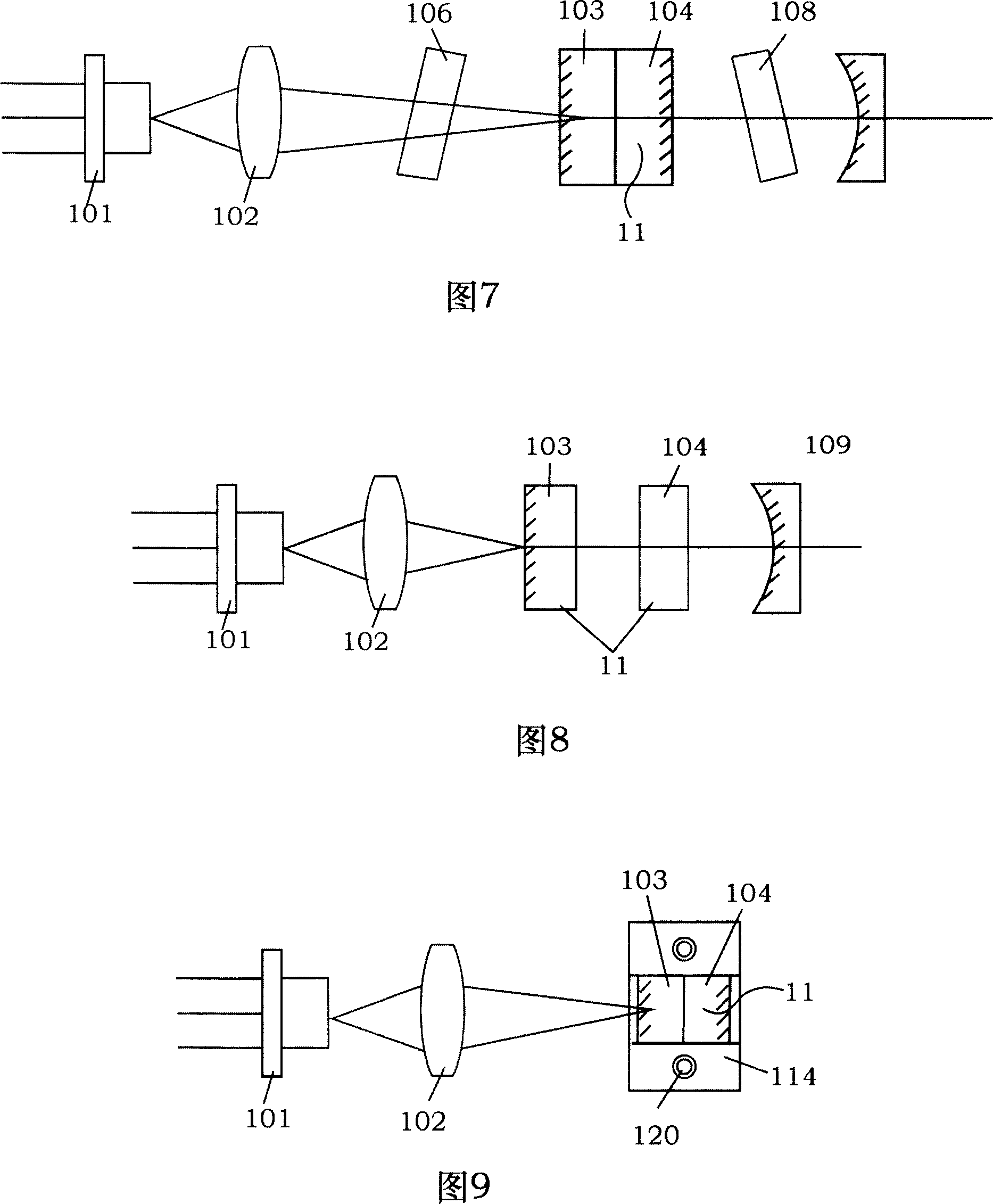
[0023] Embodiment 4: As shown in Figure 5, the first optical parallel plate 106 is inserted between the optical lens coupling system 102 and the microchip laser 11, and the pumping point is moved on the microchip laser 11. Then insert the second optical parallel plate 108, and translate the optical path back to the original output position.

[0024] Embodiment 5: As shown i...


PUM


Abstract

The invention relates to a semiconductor pumping micro laser that includes pumping source semiconductor laser, optical lens coupled system, laser gain medium and multiple frequency crystal, the laser gain medium and multiple frequency crystal are felted to form micro laser, thereinto the mode of moving pumping light as piecewise time is used to move the pumping point or micro laser which is set on the machine construction, by adopting said structure, damage area of long time working of general micro laser is little, normal damage area of micro laser is phi0.2mm, with the character of perfect uniformity of different pumping point in middle area of flat structure micro laser, the pumping is shift to prolong the life of the micro laser, so the integral life of the laser is prolonged, or using machine construction to change micro laser, the structure is simple, the realization is easy to realize, the effect of prolonging life and saving cost are also achieved.

Description

technical field [0001] The invention relates to a laser, in particular to a semiconductor pumped microchip laser. technical background [0002] At present, for microchip structure lasers, especially microchip intracavity frequency doubling lasers pumped by flat cavity end face, due to the strong laser power in the cavity, the density of laser power will gradually damage the frequency doubling crystal, thus affecting the life of the laser, as shown in Figure 1 shows a microchip laser, including a pump source semiconductor laser 101, an optical lens coupling system 102, and a laser gain medium Nd:YVO 4 103 and frequency doubling crystal KTP104, laser gain medium Nd: YVO 4 103 and the frequency doubling crystal KTP104 are connected together by bonding or gluing to form a microchip laser with a flat cavity structure. Since the frequency doubling crystal KTP104 will be gradually damaged in the long-term high-power working state, resulting in the so-called gray line, so the freq...

Claims


Application Information

Patent Timeline
Patent Type & Authority Applications(China)
IPC IPC(8): H01S3/0941H01S3/06H01S3/109H01S3/00
Inventor 吴砺凌吉武孙朝阳林斌陈卫民
Owner SHANGHAI BRANCH FUZHOU GAOYI COMM CO LTD
Why Eureka
Try Eureka