Flip chip mounting method and flip chip mounting element

A mounting method and flip-chip technology, which are applied in the manufacturing of electric solid-state devices, semiconductor devices, and semiconductor/solid-state devices, etc., can solve the problems of difficult mounting procedures, difficult conduction states, productivity or reliability residues, etc., and achieve high productivity. Effect

Active Publication Date: 2007-08-15
PANASONIC CORP
View PDF7 Cites 2 Cited by
  • Summary
  • Abstract
  • Description
  • Claims
  • Application Information

AI Technical Summary

Problems solved by technology

[0015] However, in flip-chip mounting using the above-mentioned anisotropic conductive material, electrical conduction between electrodes is obtained by mechanical contact via conductive particles, but it is difficult to obtain a stable conduction state in this way.
In addition, the conductive particles sandwiched in the counter electrode are held by the cohesive force generated by the thermosetting of the resin, so it is necessary to make the characteristics such as elastic modulus and thermal expansion coefficient of the thermosetting resin or the particle size distribution of the conductive particles consistent, Therefore, there is a problem that it is difficult to control the mounting process.
That is, in order to apply flip-chip mounting using anisotropic conductive materials to next-generation LSI chips with more than 5,000 connection terminals, there are still many problems to be solved in terms of productivity and reliability.

Method used


Image

  • Flip chip mounting method and flip chip mounting element
  • Flip chip mounting method and flip chip mounting element
  • Flip chip mounting method and flip chip mounting element

Examples


Embodiment approach 1

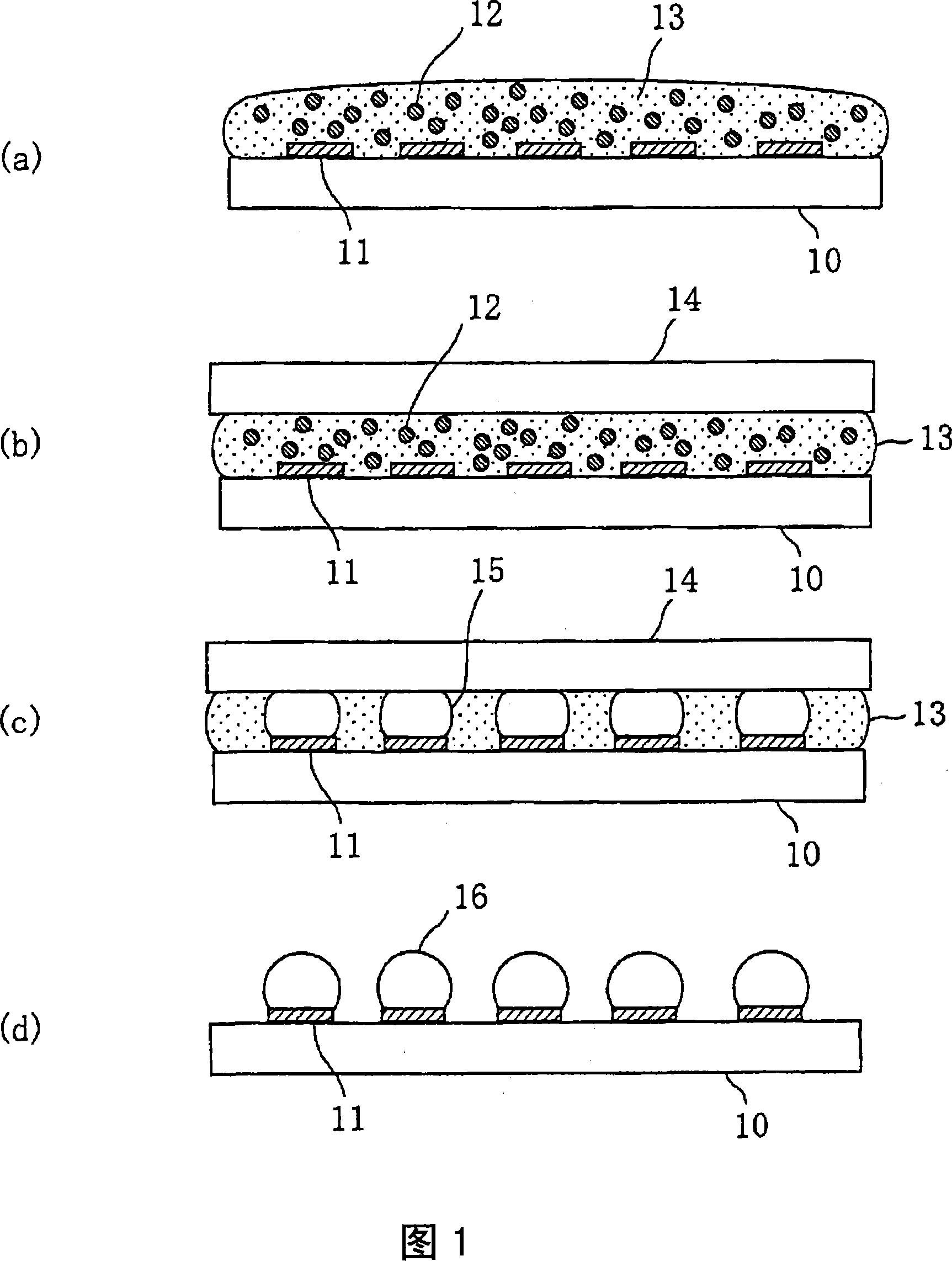
[0067] Referring to FIGS. 1( a ) to ( d ), a method of forming solder bumps according to the other flip chip mounting method will be described. As shown in FIG. 1( a ), a resin 13 containing solder powder (not shown) and a convective additive 12 is supplied on a wiring board 10 on which a plurality of electrodes 11 are formed. Next, as shown in FIG. 1( b ), while bringing the flat plate 14 into contact with the surface of the resin 13 supplied on the wiring board 10 , the wiring board 10 is heated to a temperature at which the solder powder melts. In this heating step, the melted solder powder self-assembles, and as shown in FIG. 1( c ), grown solder balls 15 are selectively formed on a plurality of electrodes 11 . Then, as shown in FIG. 1( d ), when the flat plate 14 is separated from the surface of the resin 13 and the resin 13 is removed, a wiring board 10 in which bumps 16 are formed on a plurality of electrodes 11 is obtained.

[0068] This bump forming method is charact...

Embodiment approach 2

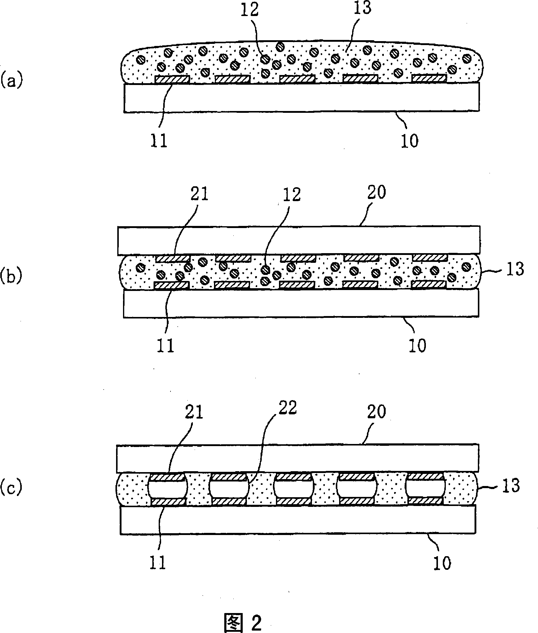
[0093] 2( a ) to ( c ) are diagrams showing basic steps of a flip chip mounting method according to Embodiment 2 of the present invention.

[0094] First, as shown in FIG. 2( a ), a resin 13 containing solder powder (not shown) and a convective additive 12 is supplied on a wiring board 10 having a plurality of electrode terminals 11 . Next, as shown in FIG. 2( b ), the semiconductor chip 20 is brought into contact with the surface of the resin 13 supplied on the wiring board 10 . At this time, the semiconductor chip 20 having a plurality of connection terminals 21 is arranged to face the wiring substrate 10 having a plurality of electrode terminals 11 . Then, in this state, wiring substrate 10 is heated to a temperature at which the solder powder melts or higher. Here, the heating temperature of the wiring board 10 is performed at the boiling point of the convection additive 12 or higher, and the boiling convection additive 12 convects in the resin 13 .

[0095] In this heat...

Embodiment approach 3

[0137] Hereinafter, Embodiment 3, which is various modifications of Embodiment 2, will be described with reference to the drawings.

[0138] Fig. 6 (a), (b) is a diagram showing the structure when a plurality of semiconductor chips (20a, 20b, 20c, 20d) are mounted on the wiring substrate 10, Fig. 6 (a) shows its top view, Fig. 6 (b) shows a cross-sectional view along line BB' of FIG. 6(a).

[0139] Flip-chip mounting of a plurality of semiconductor chips (20a, 20b, 20c, 20d) on the wiring board 10 is performed by the following method.

[0140] First, a resin containing solder powder and a convective additive is preliminarily applied to regions on the wiring board 10 where the respective semiconductor chips (20a, 20b, 20c, 20d) are mounted. Then, each semiconductor chip is brought into contact with the resin surface so that the connection terminals of the respective semiconductor chips face the respective electrode terminals on the wiring substrate 10 . Then, the wiring board...


PUM


Abstract

A flip chip mounting method, which is applicable to the flip chip mounting of the next-generation LSI and is high in productivity and reliability, comprising the steps of supplying resin (13) containing solder powder and a convective additive (12) onto a wiring board (10) having a plurality of electrode terminals (11), then bringing a semiconductor chip (20) having a plurality of connection terminals (21) into contact with the surface of resin (13), and heating the wiring board (10) to a solder powder melting temperature under this condition. The heating is conducted at a temperature higher than the boiling temperature of the convective additive (12) to allow the boiled convective additive (12) to flow throughout the resin (13). During this heating process, melted solder powder is self-assembled between the electrode terminal (11) of the wiring board (10) and the connection terminal (21) of the semiconductor chip (20) to thereby electrically connect the electrode terminal (11) with the connection terminal (21). Finally, the resin (13) is cured to fix the semiconductor chip (20) to the wiring board (10).

Description

technical field [0001] The present invention relates to a flip chip mounting method for mounting a semiconductor chip on a wiring board and a flip chip mounted body, and more particularly to high-productivity flip chip mounting that can also cope with narrower semiconductor chips Method and flip-chip mounting body. Background technique [0002] In recent years, along with the high density and high integration of semiconductor integrated circuits (LSI) used in electronic equipment, the number of pins (peen) and the narrowing of the pitch of the electrode terminals of the LSI sheet are also rapidly progressing. These LSI chips are mounted on a wiring substrate, and flip-chip mounting is widely used in order to reduce wiring delays. Furthermore, in this flip-chip mounting, generally, solder bumps are formed on the electrode terminals of the LSI chip, and electrodes formed on the wiring board are collectively bonded via the solder bumps. [0003] However, in order to mount a n...

Claims


Application Information

Patent Timeline
Patent Type & Authority Applications(China)
IPC IPC(8): H01L21/60
CPCH01L2924/14H01L2224/73204H01L2924/014
Inventor 辛岛靖治山下嘉久留河悟北江孝史中谷诚一
Owner PANASONIC CORP
Why Eureka
Try Eureka