Lithographic apparatus and device manufacturing method

A technology of optical devices and lithographic projection, which is applied in semiconductor/solid-state device manufacturing, photolithography process exposure devices, optical components, etc., and can solve the problem of inflexible generation of polarized lighting modes, impossibility, and difficulty in quickly switching lighting modes, etc. question

Active Publication Date: 2007-08-29
ASML NETHERLANDS BV
View PDF1 Cites 26 Cited by
  • Summary
  • Abstract
  • Description
  • Claims
  • Application Information

AI Technical Summary

Problems solved by technology

[0005] A possible disadvantage of conventional lithographic setups is that polarized illumination patterns (where different regions of the pupil have different polarization directions) cannot be flexibly generated
Although polarizers can be placed in the pupil plane of the illuminator, this requires expensive and bulky polarizing elements
The manipulators required for these boards are also large
In addition, specialized polarizing elements are required for several polarized illumination modes, making rapid switching of illumination modes difficult, if not impossible, during normal operation of the lithographic apparatus

Method used


Image

  • Lithographic apparatus and device manufacturing method
  • Lithographic apparatus and device manufacturing method
  • Lithographic apparatus and device manufacturing method

Examples


Embodiment Construction

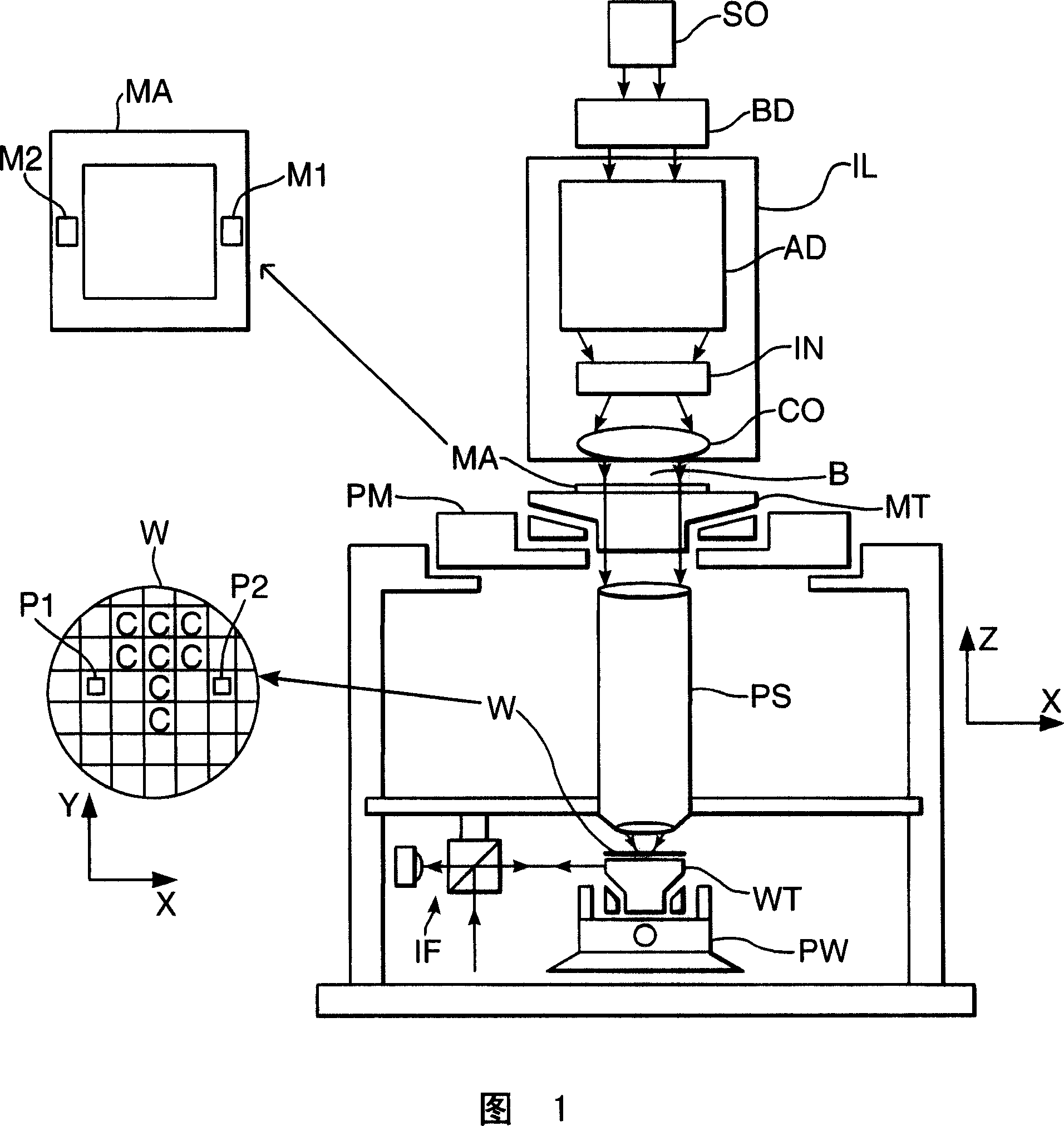
[0046] Fig. 1 schematically shows a lithographic apparatus according to an embodiment of the present invention. The unit includes:

[0047] an illumination system (illuminator) IL configured to condition a radiation beam B (eg UV radiation or DUV radiation);

[0048] a support structure (e.g. a mask table) MT configured to support a patterning member (e.g. a mask) MA and connected to a first positioner PM configured to precisely position the patterning member according to certain parameters;

[0049] A substrate table (e.g., wafer table) WT configured to hold a substrate (e.g., a resist-coated wafer) W and connected to a second positioner PW configured to precisely position the substrate according to certain parameters ;

[0050] A projection system (eg, a refractive projection lens system) PS configured to project the pattern imparted to the radiation beam B by the patterning device MA onto a target portion C of the substrate W (eg, comprising one or more chip dies).

[00...


PUM


Abstract

A lithographic projection system has an illumination system with a polarization member. A plurality of directing elements reflect different sub-beams of an incident beam into adjustable, individually controllable directions. By means of re-directing optics any desired polarized spatial intensity distribution of the beam can be produced in its cross-sectional plane.

Description

technical field [0001] The invention relates to a photolithography device and a device manufacturing method. Background technique [0002] The lithographic apparatus applies the desired pattern to the substrate, usually to a target portion of the substrate. A lithographic apparatus may be used, for example, in the manufacture of integrated circuits (ICs). In this case, a patterning device, which may also be referred to as a mask or reticle, may be used to create a circuit pattern formed on a single layer of the IC. The pattern may be transferred onto a target portion (eg comprising a portion, one or more dies) of a substrate (eg a silicon wafer). This transfer of the pattern is usually performed by imaging onto a layer of radiation sensitive material (resist) on the substrate. Typically, a single substrate contains a grid of adjacent target portions that are patterned sequentially. Known lithographic apparatuses include so-called steppers, in which the irradiation of eac...

Claims


Application Information

Patent Timeline
Patent Type & Authority Applications(China)
IPC IPC(8): G03F7/20H01L21/027H01L21/00
CPCG03F7/70191G03F7/70116G03F7/702G03F7/70566G02B27/0037
Inventor H·M·穆尔德M·F·A·尤尔林斯
Owner ASML NETHERLANDS BV
Why Eureka
Try Eureka