Thin-film transistor and thin-film transistor array base plate
A technology for thin film transistors and array substrates, applied in the field of thin film transistors, can solve problems such as voltage deviation, and achieve the effect of reducing feed-through voltage
- Summary
- Abstract
- Description
- Claims
- Application Information
AI Technical Summary
Problems solved by technology
Method used
Image

Examples
Embodiment Construction
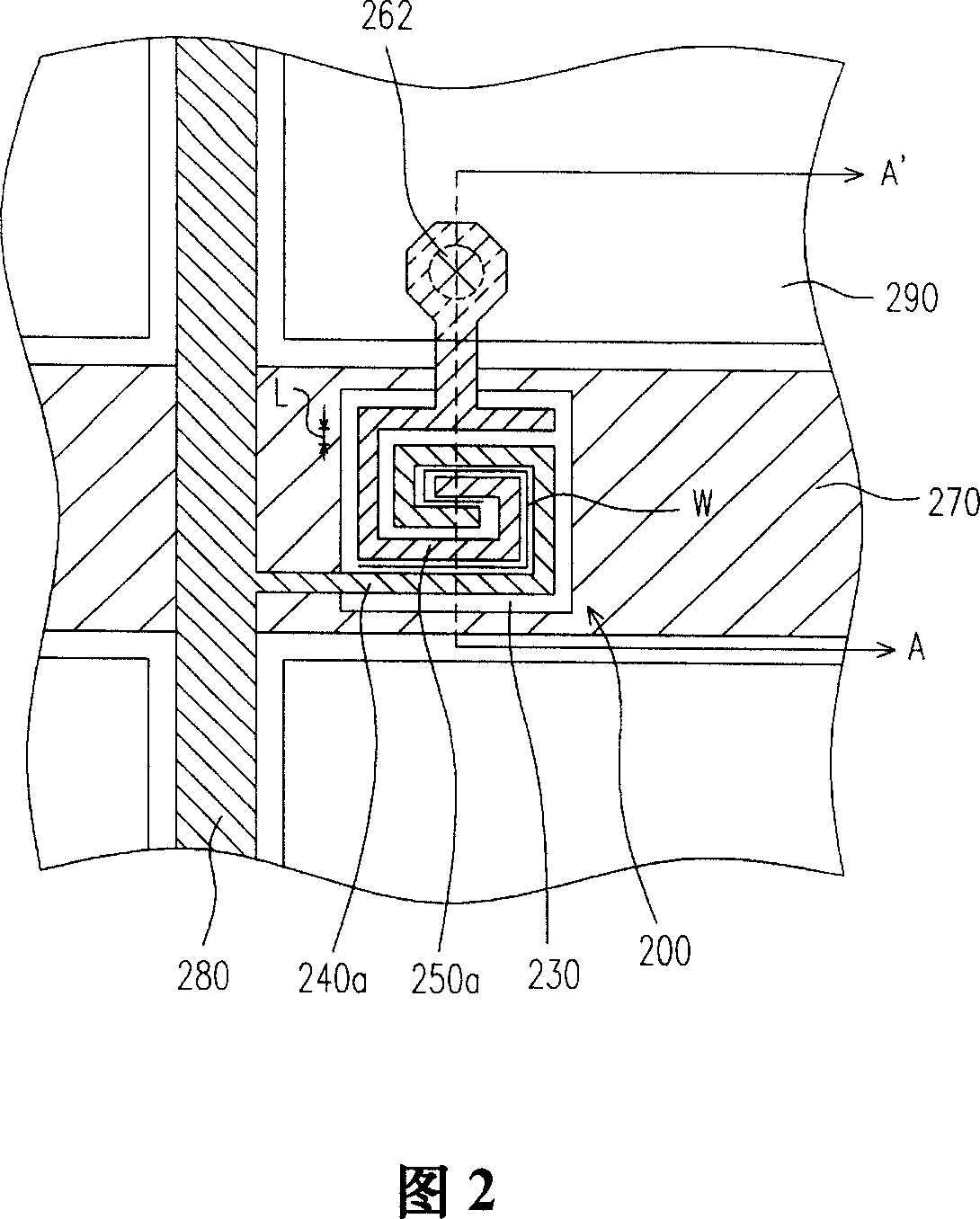
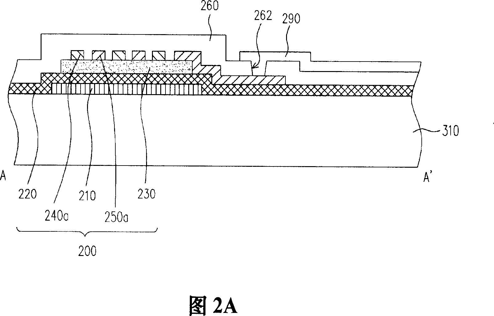
[0049] FIG. 2 is a schematic top view of a thin film transistor in a preferred embodiment of the present invention. Fig. 2A is a schematic cross-sectional view along line A-A' in Fig. 2 .
[0050]Please refer to FIG. 2 and FIG. 2A together. The thin film transistor 200 includes a gate 210 , a gate insulating layer 220 , a channel layer 230 , a spiral source 240 a and a spiral drain 250 a. The gate insulating layer 220 covers the gate 210 . The channel layer 230 is disposed on the gate insulating layer 220 above the gate 210 . The spiral source 240a is disposed on the channel layer 230 above the gate 210, and the spiral drain 250a is disposed on the channel layer 230 above the gate 210, wherein the spiral source 240a and the spiral drain 250a are wound around each other. It is set according to the state of rotation.
[0051] Referring to FIG. 2 and FIG. 2A, the thin film transistor 200, the scan line 270, the data line 280, the pixel electrode 290 and the like form a pixel s...
PUM
 Abstract
Description
Claims
Application Information
 - R&D
- Intellectual Property
- Life Sciences
- Materials
- Tech Scout
- Unparalleled Data Quality
- Higher Quality Content
- 60% Fewer Hallucinations
Browse by: Latest US Patents, China's latest patents, Technical Efficacy Thesaurus, Application Domain, Technology Topic, Popular Technical Reports.
© 2025 PatSnap. All rights reserved.Legal|Privacy policy|Modern Slavery Act Transparency Statement|Sitemap|About US| Contact US: help@patsnap.com